-
-
News
News Highlights
- Books
Featured Books
- pcb007 Magazine
Latest Issues
Current IssueThe Hole Truth: Via Integrity in an HDI World
From the drilled hole to registration across multiple sequential lamination cycles, to the quality of your copper plating, via reliability in an HDI world is becoming an ever-greater challenge. This month we look at “The Hole Truth,” from creating the “perfect” via to how you can assure via quality and reliability, the first time, every time.
In Pursuit of Perfection: Defect Reduction
For bare PCB board fabrication, defect reduction is a critical aspect of a company's bottom line profitability. In this issue, we examine how imaging, etching, and plating processes can provide information and insight into reducing defects and increasing yields.
Voices of the Industry
We take the pulse of the PCB industry by sharing insights from leading fabricators and suppliers in this month's issue. We've gathered their thoughts on the new U.S. administration, spending, the war in Ukraine, and their most pressing needs. It’s an eye-opening and enlightening look behind the curtain.
- Articles
- Columns
- Links
- Media kit
||| MENU - pcb007 Magazine
High Density Packaging User Group Announces Mitsui Mining & Smelting Membership
November 11, 2022 | HDP User GroupEstimated reading time: Less than a minute

High Density Packaging (HDP) User Group is pleased to announce that Mitsui Mining & Smelting Co., LTD. (Mitsui Kinzoku) has become a member.
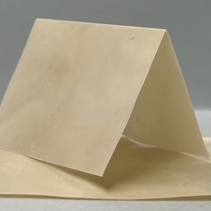
Mitsui Kinzoku has been contributing to worldwide society by providing various valuable products. One of those products is copper foil. The company focuses primarily on high-end applications in each electronics field, such as advanced packaging and high-speed communications. The company expects that their materials knowledge will be utilized in several HDP projects.
“I am pleased to welcome Mitsui Kinzoku to HDP, joining the outstanding companies working on HDP User Group projects. Their expertise and capability in high-performance copper foil, especially for high-frequency and high-speed applications, will contribute significantly to several of our emerging technology projects”, said Larry Marcanti, Executive Director of HDP User Group.
Suggested Items
The Evolution of Picosecond Laser Drilling
06/19/2025 | Marcy LaRont, PCB007 MagazineIs it hard to imagine a single laser pulse reduced not only from nanoseconds to picoseconds in its pulse duration, but even to femtoseconds? Well, buckle up because it seems we are there. In this interview, Dr. Stefan Rung, technical director of laser machines at Schmoll Maschinen GmbH, traces the technology trajectory of the laser drill from the CO2 laser to cutting-edge picosecond and hybrid laser drilling systems, highlighting the benefits and limitations of each method, and demonstrating how laser innovations are shaping the future of PCB fabrication.
Day 2: More Cutting-edge Insights at the EIPC Summer Conference
06/18/2025 | Pete Starkey, I-Connect007The European Institute for the PCB Community (EIPC) summer conference took place this year in Edinburgh, Scotland, June 3-4. This is the third of three articles on the conference. The other two cover Day 1’s sessions and the opening keynote speech. Below is a recap of the second day’s sessions.
Day 1: Cutting Edge Insights at the EIPC Summer Conference
06/17/2025 | Pete Starkey, I-Connect007The European Institute for the PCB Community (EIPC) Summer Conference took place this year in Edinburgh, Scotland, June 3-4. This is the second of three articles on the conference. The other two cover the keynote speeches and Day 2 of the technical conference. Below is a recap of the first day’s sessions.
Preventing Surface Prep Defects and Ensuring Reliability
06/10/2025 | Marcy LaRont, PCB007 MagazineIn printed circuit board (PCB) fabrication, surface preparation is a critical process that ensures strong adhesion, reliable plating, and long-term product performance. Without proper surface treatment, manufacturers may encounter defects such as delamination, poor solder mask adhesion, and plating failures. This article examines key surface preparation techniques, common defects resulting from improper processes, and real-world case studies that illustrate best practices.
RF PCB Design Tips and Tricks
05/08/2025 | Cherie Litson, EPTAC MIT CID/CID+There are many great books, videos, and information online about designing PCBs for RF circuits. A few of my favorite RF sources are Hans Rosenberg, Stephen Chavez, and Rick Hartley, but there are many more. These PCB design engineers have a very good perspective on what it takes to take an RF design from schematic concept to PCB layout.