-
- News
- Books
Featured Books
- design007 Magazine
Latest Issues
Current IssueLevel Up Your Design Skills
This month, our contributors discuss the PCB design classes available at IPC APEX EXPO 2024. As they explain, these courses cover everything from the basics of design through avoiding over-constraining high-speed boards, and so much more!
Opportunities and Challenges
In this issue, our expert contributors discuss the many opportunities and challenges in the PCB design community, and what can be done to grow the numbers of PCB designers—and design instructors.
Embedded Design Techniques
Our expert contributors provide the knowledge this month that designers need to be aware of to make intelligent, educated decisions about embedded design. Many design and manufacturing hurdles can trip up designers who are new to this technology.
- Articles
- Columns
Search Console
- Links
- Events
||| MENU - design007 Magazine
IPC Training Course on PCB Design for RF Boards
July 26, 2023 | IPCEstimated reading time: Less than a minute
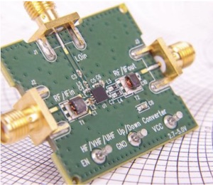
IPC will be holding a training course on printed circuit board (PCB) design for radio frequency (RF) board every Mondays and Wednesday from August 7 to September 13. The training sessions will be held via virtual meetings 11am to 1pm ET (5-7pm CET).
The program is designed to provide circuit board designers with a balanced foundation of theoretical knowledge and practical skills in printed circuit board design.
Upon completion, participants will be able to design boards for high-speed analog and RF/microwave frequencies; understand the trade-offs in materials used in these applications; define a board stackup that implements structures that will meet the needs of these designs; as well as understand and mitigate signal integrity issues for these designs.
They will also be able to learn the effects of mechanical retention needs for these applications, define and implement the tighter manufacturing tolerances, as well as understand the documentation requirements for these designs.
For more information, visit www.ipc.org.
Suggested Items
Connect the Dots: Designing for Reality—The Pre-Manufacturing Process
05/08/2024 | Matt Stevenson -- Column: Connect the DotsI have been working with Nolan Johnson on a podcast series about designing PCBs for the reality of manufacturing. By sharing lessons learned over a long career in the PCB industry, we hope to shorten learning curves and help designers produce better boards with less hassle and rework. Episode 2 deals with the electronic pre-manufacturing process. Moving from CAD (computer-aided design) to CAM (computer-aided manufacturing) is a key step in PCB manufacturing. CAM turns digital designs into instructions that machines can use to actually build the PCB.
Indium Corporation to Showcase HIA Materials at ECTC
05/07/2024 | Indium CorporationAs an industry leader in innovative materials solutions for semiconductor packaging and assembly, Indium Corporation® will feature its advanced products designed to meet the evolving challenges of heterogeneous integration and assembly (HIA) and fine-pitch system-in-package (SiP) applications at the 74th Electronic Components and Technology Conference (ECTC), May 28‒31, in Denver, Colorado.
Siemens Delivers New Solido IP Validation Suite
05/07/2024 | SiemensSiemens Digital Industries Software introduced Solido™ IP Validation Suite software, a comprehensive, automated signoff solution for quality assurance across all design intellectual property (IP) types, including standard cells, memories and IP blocks.
Altair Acquires Research in Flight, Forging a New Path for Aerodynamic Analysis
05/07/2024 | AltairAltair a global leader in computational intelligence, announced it has acquired Research in Flight, maker of FlightStream®, which provides computational fluid dynamics (CFD) software with a large footprint in the aerospace and defense sector and a growing presence in marine, energy, turbomachinery, and automotive applications.
Happy’s Tech Talk #28: The Power Mesh Architecture for PCBs
05/07/2024 | Happy Holden -- Column: Happy’s Tech TalkA significant decrease in HDI substrate production cost can be achieved by reducing the number of substrate layers from conventional through-hole multilayers and microvia multilayers of eight, 10, 12 (and more), down to four. Besides reducing direct processing steps, yield will increase as defect producing operations are eliminated.