


 The Chemical Connection: Onshoring PCB Production—Daunting but Certainly Possible
 It’s Only Common Sense: The Phone Is Still Mightier Than the Keyboard


StenTech Discusses Revolution of Stencil Manufacturing with Laser Technology at SMTA Guadalajara
September 25, 2023 | StenTechEstimated reading time: 1 minute
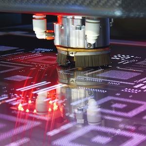
StenTech Inc., the leading multinational SMT Printing Solutions company, is pleased to announce plans to exhibit at the SMTA Guadalajara Expo, scheduled to take place Oct. 25-26, 2023 at the Expo Guadalajara in Guadalajara, Jalisco, Mexico. This year's exhibition promises to be a game-changer as StenTech unveils its latest capabilities, including a state-of-the-art laser system and award-winning Advanced Nano Coating in Booth 920.
StenTech has raised the bar in the stencil manufacturing industry by making a substantial investment in the newest iteration of the StencilLaser G6080 from LPKF Laser & Electronics. This cutting-edge laser system represents a significant milestone for the SMT industry in Mexico, showcasing StenTech's unwavering commitment to its esteemed local customer base in Jalisco.
The StencilLaser G6080 stands as a flagship laser system, renowned for its best-in-class technology, tailored to meet the exacting demands of even the most discerning stencil users in the SMT industry. Distinguished by its custom carbon fiber architecture, this state-of-the-art laser system ensures superior positioning accuracy and sidewall quality while maximizing productivity. Versatile and adaptable, it is capable of cutting stainless steel and nickel stencils with material thicknesses ranging from 20 um to 1 mm (0.8 to 40 mil). StenTech's investment in this advanced laser technology empowers the company to deliver stencil solutions that consistently meet the highest industry standards.
In addition to its latest investment in state-of-the-art laser technology, StenTech's Guadalajara facility also offers an array of cutting-edge capabilities, including Advanced Nano Coating, tooling solutions, and unparalleled customer service. The combination of these advanced offerings positions StenTech as a trusted partner for the most demanding stencil projects, meeting the unique needs of its customers across various industries.
The Advanced Nano Coating features an exceptional 1-3 um hardened nano coating expertly applied to the bottom side and inside the apertures of the stencil. This cutting-edge technology offers remarkable anti-adhesion properties, effectively repelling solder flux and ensuring superior paste transfer.
By harnessing the power of StenTech's Advanced Nano Coating, transfer efficiency can soar by up to 25 percent, resulting in a substantial reduction in bridging and paste-related defects. The "non-stick" characteristics of the coating also lead to reduced underside cleaning, contributing to improved yields and decreased expenses on rework and touch-up. Additionally, stencils coated with Advanced Nano are ready for use just 30 minutes after coating, elevating production efficiency and minimizing downtime.
Share on:


Testimonial
"Your magazines are a great platform for people to exchange knowledge. Thank you for the work that you do."
Simon Khesin - Schmoll MaschinenSuggested Items
TSMC Reports Third Quarter EPS of NT$17.44
10/22/2025 | TSMCTSMC announced consolidated revenue of NT$989.92 billion, net income of NT$452.30 billion, and diluted earnings per share of NT$17.44 (US$2.92 per ADR unit) for the third quarter ended September 30, 2025.
MKS’ Atotech, ESI to Participate in TPCA Show & IMPACT Conference 2025
10/17/2025 | MKS’ AtotechMKS Inc., a global provider of enabling technologies that transform our world, announced that its strategic brands Atotech (process chemicals, equipment, software, and services) and ESI (laser systems) will showcase their latest range of leading manufacturing solutions for printed circuit board (PCB) and package substrate manufacturing at the upcoming 26th TPCA Show 2025 to be held at the Taipei Nangang Exhibition Center from 22-24 October 2025.
I-Connect007 Editor’s Choice: Five Must-Reads for the Week
10/17/2025 | Marcy LaRont, I-Connect007Much of the news over the last week focused on the push-pull between the U.S. and China and the latter’s most recent announcement about rare earth mineral restrictions. Despite that situation, the IMF raised its growth forecast, and global markets showed cautious optimism. Then, as the U.S. attempted to retreat from all environmentally based policy and ESG gains achieved to date, the global shipping emissions pact continues to gain momentum.
ASC Sunstone Circuits Adds New Options to OneQuote While Maintaining Real-Time Pricing on Core PCB Features
10/16/2025 | ASC Sunstone CircuitsASC Sunstone Circuits, a leading U.S. PCB manufacturer, today announced a significant expansion of its OneQuote online quoting tool, giving design engineers more control over complex PCB configurations — making it easier for the quote team to quickly clarify and verify specifications, reducing delays from manual quote reviews.
HT Global Circuits Adds Two atg Luther & Maelzer Flying Probe Test Systems
10/15/2025 | atg Luther & Maelzer GmbHAtg Luther & Maelzer GmbH, a leading supplier of electrical testing solutions for the PCB industry, and IEC USA, a distributor of consumables, equipment, and services in the North American PCB market, confirm the order for high-speed bare board testing technology.