


 The Government Circuit: New Council Now Helps Shape Policy Decisions in the Electronics Supply Chain
 Learning With Leo: Soldering—The Interpretation Problem
 Nolan’s Notes: The ROI of Setup Optimization


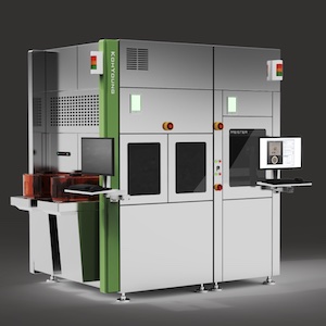
Koh Young Technology, the leader in True3D™ measurement-based inspection solutions, will be speaking at the SMTA Wafer-Level Packaging Symposium in Burlingame, California on our Multimodal Phase Shift Optics Approach to revolutionize high-speed 3D reconstruction of semiconductor and advanced packages. In the presentation will highlight how high-speed 3D reconstruction addresses the growing demand for electronic components, which necessitates fast and efficient processing. These advancements in measurement technology and AI integration have paved the way for enhanced packaging applications in the semiconductor industry.
During the event on Tuesday, 13 February 2024, Dr. Seung Hyun Lee, Ph.D. will present the paper “High-Speed Die and Component 3D Reconstruction Solution by Multimodal Phase Shift Optics Approach”. Therein he will explain how advancements in optical 3D measurement and the integration of Artificial Intelligence (AI) have paved the way for advanced packaging applications. Multi-modal measurement probes, equipped with enhanced depth of focus, can cover height differences in the latest package designs. Various surface conditions of components, chips, and surfaces are measured by combining an oblique optical system, which ensures stable high-speed measurement of objects with diffuse reflection, with a coaxial optical system, suitable for measuring objects with specular reflection. The integration of AI deep learning technology enables effective processing of various noises encountered during the measurements.
The SMTA WLPS will explore the massive changes in advanced package technology because electrical system architects are directly driving package performance requirements, something which has never happened before. Previously System Architects designed circuits around package limitations because pushing package technologies outside of their “comfort zones” often led to undesirable results. With the rise in transistor costs and the need to improve power efficiency, Silicon Architects have little choice but to push advanced package technologies well beyond their comfort zones.
The Wafer-Level Packaging Symposium will bring together the semiconductor industry’s most respected authorities to address all aspects of wafer-level, 3D device packaging, advanced manufacturing & test technologies. Addressing wafer-level packaging, 3D, and Advanced Manufacturing & Test technologies, the Wafer-Level Packaging Symposium will be at the forefront of packaging technology evolution. The conference will feature attendees from around the globe in the heart of Silicon Valley to immerse themselves in the latest technology and business trends. Register today at www.smta.org/mpage/wafer-register.
Other content from Koh Young:
- The Printed Circuit Assembler’s Guide to… SMT Inspection: Today, Tomorrow, and Beyond by Brent Fischthal. (Download the companion guide here.)
- I-007e Micro Webinar Series: “Smarter Manufacturing Enabled with Inspection Data” by Joel Scutchfield
You can view other titles in the I-007eBooks library here.


