


 Elementary, Mr. Watson: Heat—The Hidden Villain of Power Electronics
 Beyond Design: The Fundamental Structure of Spectral Integrity
 The Shaughnessy Report: Watt About Power Integrity?


Combine Aven’s Cyclops and Inspector Lamp for Unprecedented Detail in Cable Wire Harness Applications
January 29, 2024 | AvenEstimated reading time: 1 minute
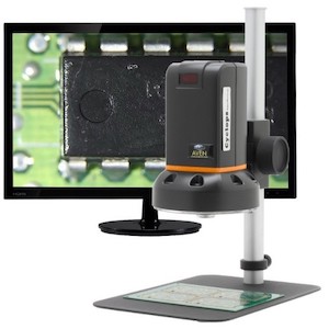
Aven, a full-service technology provider, is pleased to offer an advanced solution for harness and cable wiring applications by combining the Cyclops HDMI Digital Microscope with the versatile Inspector Lamp. This integration offers operators convenience and precision in inspection processes.
The Cyclops sets a new standard in inspection scopes with a 4x Lens. This innovative tool connects directly to a monitor through a 1080p HDMI output, providing operators with high-quality, real-time images on a large screen. The 21.5" HD monitor offers a comfortable and ergonomic viewing experience, eliminating the need to hunch over narrow microscope eyepieces.
With an exceptional working distance, the Cyclops allows operators to examine objects of various sizes with ease. The magnification ranges up to 132x, delivering stunning images for detailed inspection. The 2-megapixel sensor ensures exceptionally crisp and high-resolution visuals, enhancing the precision of inspection tasks.
The Cyclops Digital Microscope Cyclops can be used alongside the Inspector Lamp, providing versatile lighting options for different applications. 30 LED lights with adjustable intensity control allows operators to control the brightness and optimize lighting conditions for accurate inspections.
"By implementing the Cyclops HDMI along with our Inspector Lamp, we are offering a comprehensive solution for harness and cable wiring applications. This not only provides exceptional image quality but also ensures operators have flexible lighting options to enhance their inspection processes," said Mark Kanpurwala, VP Sales & Marketing at Aven.
Aven continues to push the boundaries of innovation in the optical and ergonomic tools industry, providing professionals with cutting-edge solutions for their inspection and precision needs. The company manufactures and distributes a range of high-performance, optical instruments and precision tools for microscopy, inspection and assembly.
Share on:


Testimonial
"We’re proud to call I-Connect007 a trusted partner. Their innovative approach and industry insight made our podcast collaboration a success by connecting us with the right audience and delivering real results."
Julia McCaffrey - NCAB GroupSuggested Items
Koh Young Unveils Breakthrough Innovations at Productronica and SEMICON Europa 2025
10/28/2025 | Koh YoungKoh Young, the industry leader in True 3D measurement-based inspection and metrology solutions, will showcase a wave of innovations at Productronica and SEMICON Europa 2025, taking place November 18–21 at Messe München, Germany.
New Episode of Voices of the Industry Podcast Explores Breakthroughs in Test and Inspection
10/22/2025 | I-Connect007In this episode of Voices of the Industry, “Testing Innovation: Advances in Test, Inspection & Failure Analysis,” host Nolan Johnson speaks with Rob Boguski, president of Datest. Together, they explore the expanding world of circuit testing, inspection, and failure analysis, areas that are experiencing a surge in technological capability and sophistication. As Johnson and Boguski discuss, today’s test companies are performing analyses and precision methods that would have seemed impossible just a decade ago.
Knocking Down the Bone Pile: Revamp Your Components with BGA Reballing
10/14/2025 | Nash Bell -- Column: Knocking Down the Bone PileBall grid array (BGA) components evolved from pin grid array (PGA) devices, carrying over many of the same electrical benefits while introducing a more compact and efficient interconnect format. Instead of discrete leads, BGAs rely on solder balls on the underside of the package to connect to the PCB. In some advanced designs, solder balls are on both the PCB and the BGA package. In stacked configurations, such as package-on-package (PoP), these solder balls also interconnect multiple packages, enabling higher functionality in a smaller footprint.
Koh Young Discussing Ways to Apply Smart Factory Insights to Maximizing Productivity at SMTA Tijuana
10/14/2025 | Koh YoungKoh Young, the industry leader in True 3D measurement-based inspection solutions, will present at the SMTA Tijuana Expo & Tech Forum on November 13, 2025, at the Quartz Hotel in Tijuana, Baja California.
The Training Connection, LLC Welcomes Industry Veteran Jack Harris to Lead Training Partnerships
10/07/2025 | The Training Connection LLCThe Training Connection, LLC (TTC-LLC), a premier provider of test engineering and development training, is proud to announce that Jack Harris, one of the most recognized names in electronics manufacturing training and technical development, has joined the company as Relationship Lead, Training.