


 Learning With Leo: UHDI—The Next Leap in PCB Manufacturing
 Nolan’s Notes: Is Mexico the Pulse of Electronics in the Americas?
 Standard of Excellence: Speed vs. Quality in Customer Service


MS2 a Beneficial System for Reducing Solder Dross
April 4, 2024 | I-Connect007 Editorial TeamEstimated reading time: 2 minutes
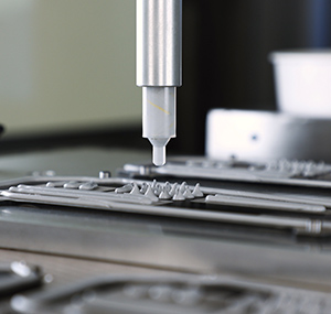
We recently spoke with Octavio Raygoza, sales manager for P Kay Metal in Mexico, to discuss how P.Kay’s MS2® system for reducing solder dross is both financially and environmentally responsible. By reducing solder dross up to 85%, you nearly double the output while consuming the same amount of solder.
Nolan Johnson: Welcome, Octavio. It’s great to talk with you. What does MS2 do in the manufacturing process?
Octavio Raygoza: MS2 is a chemistry solution that helps reduce solder dross by up to 85%. It works on tin-lead and lead free alloys in your wave solder machinery. MS2 Molten Solder Surfactant does not change or affect the solder alloy in your pot; MS2 has no odor and is not toxic; and it is environmentally friendly (LF version is 100% RoHS-compliant).
Barry Matties: One of the financial advantages to MS2 is lowering hazardous waste costs, but it also reduces new solder usage, which is a cost reduction. Considering you’re reducing solder usage up to 85%, that seems profitable and sustainable. What about sustainability?
Raygoza: When companies decide to use MS2, they obtain big savings, making it easy to pay for the offline solder dross recovery equipment. They can make the investment, and the ROI is quick—approximately three to five months.
Matties: From the green and sustainability aspects, you're saving all the shipping, storage, and handling for both solder and solder dross. But does sustainability also include reducing or eliminating solder defects and rework?
Raygoza: When the solder in the bath gets contaminated, that contamination causes voids. A small part of oxide in the solder affects the quality. When we remove the oxide, the quality is better.
Johnson: This is very compelling with regard to running your wave solder machines since 85% means that you nearly double the output while consuming the same amount of solder. The MS2 process is economically and environmentally sustainable, and you have effects like reduced transportation costs for the waste from before.
Raygoza: This is a good point. Recycling income is in the sustainability plan.
Matties: As technology requires finer lines and tighter features, having a solder bath as clean as an MS2 bath is a huge advantage in capability and quality, as well as reduced solder consumption.
When you can eliminate 85% of the waste from your solder usage, that's amazing. That should translate into sales right from the beginning. What is the return on investment?
Raygoza: It depends on the volume of the company, but you see ROI from the very first liter. Customers save approximately $2,000 per liter when working with the most expensive lead-free alloys.
Matties: When somebody decides to implement this, Octavio, how rapidly will they see this operating in their facility? Is it a long startup process?
Raygoza: The process starts as soon as the customer places their first MS2 order.
Johnson: Octavio, thank you for explaining the benefits of P.Kay’s MS2 Molten Solder Surfactant for both tin-lead and lead-free alloys. It sounds like you can’t go wrong.
Raygoza: Of course, Nolan. I agree.
Share on:


Testimonial
"The I-Connect007 team is outstanding—kind, responsive, and a true marketing partner. Their design team created fresh, eye-catching ads, and their editorial support polished our content to let our brand shine. Thank you all! "
Sweeney Ng - CEE PCBSuggested Items
Mycronic Unveils BA 01 Small Dot Ejector for Next-Generation Precision Jet Printing
11/12/2025 | MycronicMycronic’s BA 01 small dot ejector, delivers unmatched precision in solder paste jet printing for advanced PCB designs.
Indium is Electrifying the Future with Advanced Materials Solutions at productronica
11/11/2025 | Indium CorporationAs one of the leading providers in advanced materials solutions for power device packaging and materials for the electronics assembly and solder industries, Indium Corporation® is proud to feature its lineup of high-reliability products at Productronica, taking place November 18-21, in Munich, Germany.
KOKI to Host Technical Webinar on Dewetting Defects in SMT Soldering
11/11/2025 | KOKIKOKI, a global leader in advanced soldering materials and process solutions, announced its upcoming technical webinar, “Understanding and Preventing Dewetting Defects in SMT Soldering.”
Discover the Benefits of Inkjet with Electra Polymer at Productronica 2025
11/10/2025 | Electra Polymers LtdElectra Polymers will be showcasing ElectraJet® EMJ110, our advanced low-loss inkjet soldermask, ideal for high-speed and high-frequency PCB applications, at productronica 2025.
Redefining Solder Paste Application – Essemtec Reaches 1.1 Million Dots per Hour
11/06/2025 | EssemtecEssemtec, the Swiss manufacturer of adaptive SMT and dispensing solutions, announces a major performance upgrade to its Jet-on-the-Fly High Speed solder paste jetting technology, now achieving 1.1 million dots per hour.