


 Beyond Design: AI-driven Inverse Stackup Optimization
 Global PCB Connections: Following DFM Rules Leads to Better Boards
 Elementary Mr. Watson: How to Reinvent Your Professional Journey


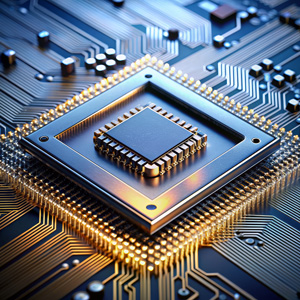
LPKF is Ready for Increasing Demand for Glass Substrates in the Semiconductor Industry
May 13, 2024 | LPKFEstimated reading time: 2 minutes
The semiconductor industry is shifting towards glass to package the most advanced semiconductor chips. LPKF’s mature LIDE technology is enabling that transition into this new era from ramp-up to high volume manufacturing.
Major changes in the semiconductor market
New developments in data center, and automotive markets require new semiconductor solutions. This market demand is driven by trends like high performance computing, remote working, Artificial Intelligence, and self-driving cars.
Major challenges for the semiconductor industry are the competitive price levels to produce semiconductor solutions, differentiation in the supply chains and new requirement due to changing markets. The semiconductor market is therefore evolving constantly.
Major global players introduced glass as promising new solution to address industrial needs in high performance computing and AI applications. They recently announced that glass substrates will become the new market standard.
Advanced packaging with glass substrates
Moore’s law is slowing down. The semiconductor industries solutions to compensate this slowdown are advanced packaging and heterogenous integration. This is reached by using different chips manufactured with different advanced manufacturing processes.
One future building block for advanced packaging and heterogeneous integrations is glass as the substrate material. It serves as a solution to overcome packaging challenges with materials like silicon and glass fiber reinforced plastics.
Since many years, LPKF has invested into research, processes, and product development and reached an outstanding level of maturity to provide production capabilities for high-volume manufacturing. “Our technology reached an outstanding level of maturity to meet the semiconductor industry’s needs. For that reason, we increased our production capacities in 2024 to satisfy the increasing customer demand.” states Klaus Fiedler, CEO of LPKF.
In the past 10 years, LPKF has developed its industrial processes for glass manufacturing using highest quality standards and with focus on throughput to reach industrial requirements. The LIDE process (Laser Induced Deep Etching) developed by LPKF is well established. Glass substrates from 100µm up to 1.1mm can be processed quickly, precisely, and without damage such as microcracks. This is essential for the scalability, reliability, and cost efficiency of the electronic package.
High process maturity of LPKF technology
High process maturity and tangible operational proof of performance convinced global players to collaborate with LPKF. LPKF supports customers throughout the adoption of glass core for advanced packaging application by integrating the technology into customers manufacturing processes or providing manufacturing service by its Vitrion division. With dozens of worldwide installed tools and thousands of manufactured glass substrates in LPKF’s own manufacturing facility, LPKF gave proof of the maturity of the technology.
“Global players value the high precision, flexibility and design freedom of LIDE technology.” underlines Dr. Roman Ostholt, Managing Director Electronics. LPKF’s long-lasting experience and presence on the market is an additional plus. This is the reason for being a reliable partner and the increasing demand in LPKF’s technological solutions from the semiconductor industry.
Outstanding know-how and quality, the capacity to satisfy the market demand and to support industry partners in making the step into using glass substrates in the semiconductor industry makes LPKF to a reliable global partner.
Share on:


Suggested Items
Mycronic Receives $6-8 Million SLX Mask Writer Order
12/26/2024 | MycronicMycronic AB has received an order for an SLX mask writer from an existing customer in Asia. The order value is in the range of $6 to $8 million. Delivery of the system is planned for the first quarter of 2026.
SIA Statement on Biden Administration’s Launch of Section 301 Trade Investigation Related to China’s Targeting of the Semiconductor Industry for Dominance
12/25/2024 | SIAThe Semiconductor Industry Association (SIA) released the following statement from SIA President and CEO John Neuffer regarding the Biden administration’s decision to launch a Section 301 trade investigation focused on China’s acts, policies, and practices related to targeting of the semiconductor industry for dominance.
Biden-Harris Administration Announces CHIPS Incentives Award with Texas Instruments to Expand U.S. Capacity of Current-Generation and Mature-Node Chips
12/23/2024 | U.S. Department of CommerceThe Biden-Harris Administration announced that the U.S. Department of Commerce awarded Texas Instruments (TI) up to $1.61 billion in direct funding under the CHIPS Incentives Program’s Funding Opportunity for Commercial Fabrication Facilities.
Biden-Harris Administration Announces CHIPS Incentives Award with Samsung Electronics to Solidify U.S. Leadership in Leading-Edge Semiconductor Production
12/23/2024 | U.S. Department of CommerceThe Biden-Harris Administration announced that the U.S. Department of Commerce awarded Samsung Electronics (Samsung) up to $4.745 billion in direct funding under the CHIPS Incentives Program’s Funding Opportunity for Commercial Fabrication facilities.
SIA Praises Finalization of CHIPS Incentives to Supplement SK Hynix’s $3.87 Billion Investment in Indiana
12/20/2024 | SIAThe Semiconductor Industry Association (SIA) today released the following statement from SIA President and CEO John Neuffer commending finalization of CHIPS and Science Act manufacturing investments announced by the U.S. Department of Commerce and SK hynix. The incentives will supplement the company’s $3.87 billion investment in Indiana for advanced packaging operations and R&D.