


 Connect the Dots: Designing for Reality: Outer Layer Imaging
 Elementary, Mr. Watson: The Paradigm Shift of Silicon-to-System Design
 Fresh PCB Concepts: The Journey of a PCB—A Tale of Sustainability and Circularity
Unique Look Behind the Scenes of AT&S Research
May 23, 2024 | AT&SEstimated reading time: 3 minutes
The technology leader AT&S already holds almost 800 patents and is giving an insight into its R&D departments in Leoben at the “Long Night of Research” on May 24. But some things remain top secret: the new research center and Europe’s first substrate plant recently installed a high-tech machine that is unique in the world. It allows the exposure of substrate structures that are 14 times thinner than a human hair.
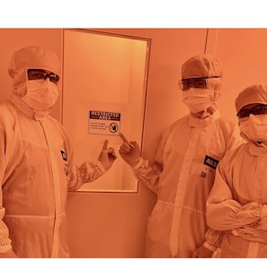
“No photography” and “Restricted Area” – as if these signs weren’t enough, the high-tech machine is also concealed behind a plastic screen. What stands here in the protective yellow light of the clean room is the pride and joy of the R&D team at the new substrate research center “HTB3” in Leoben.
From the outside, the cube-shaped machine is inconspicuous. And yet: there is no other machine like it in the world and it would cost several million euros to buy – but AT&S has been provided with it by the manufacturer as a prototype for six months for testing purposes. This provides the production company with practical data to make the device ready for series production, and the AT&S engineers have a special tool to carry out invaluable R&D analyses in parallel with production.
The inner workings are spectacular: the machine is an exposure tool for lithography, a so-called Direct Imager, which can expose extremely fine structures in substrate production. In microtechnology, the micrometer is the measure of all things: 1 micrometer (1 μm) is a thousandth of a millimeter. The conductor tracks that can be produced using this exposure device are only 5 μm wide (0.005 mm). By comparison, a human hair is around 70 μm thick (0.07 mm) – and therefore 14 times wider.
The team led by Leoben R&D expert Timo Schwarz has been testing the Direct Imager since May and has carried out countless analyses. The new R&D tool enables a high resolution in combination with greater depth of field, generally more configuration options, unlimited design variations and a faster, more flexible and resource-saving test phase compared to other technologies. “For the first time in Europe, we are researching the further development of our IC substrate technology under near-production conditions, creating added value for us and our partners,” Schwarz is proud of the development in Leoben.
What are substrates?
In simple terms, substrates are reduction couplings from printed circuit boards to the chip. They connect the tiny inputs and outputs of powerful microchips (such as in graphics cards) with the much larger structures of the printed circuit board. Today, substrates are an important basis for all forms of data processing. AT&S already holds almost 800 patents for the manufacture of IC substrates and high-tech printed circuit boards. More than a fifth of the company’s turnover is the result of the innovative strength of AT&S research. “The fact that we not only support top customers with AT&S, but are even development partners for many of them, shows the trust and appreciation that we enjoy with our technological excellence,” says AT&S Head of Research Hannes Voraberger. “Especially in Europe, a focus on research and development of highly complex microelectronics is essential to avoid becoming economically and technologically dependent.”
AT&S CTO Peter Griehsnig also emphasizes the aspects of sustainability: “AT&S’s R&D activities contribute to sustainable development in two ways: Firstly, innovative tools in research work save valuable amounts of time, costs and materials, and secondly, the products created with them ensure more efficient data transmission and smart, green energy efficiency for our end customers.”
Share on:


Suggested Items
I-Connect007 Editor’s Choice: Five Must-Reads for the Week
09/27/2024 | Nolan Johnson, I-Connect007If you know Dave Hoover of TTM, then I am honored to inform you that he has retired from the industry as of this week. But we can keep tabs on him through his weekly online blues radio program “Groovy Hoovy’s Different Shades of Blue Radio and Video Show.” Congratulations on your transition to “civilian” life, Dave.
Welcome Day: AT&S Trains 21 New Apprentices for the High-tech Industry
09/26/2024 | AT&SNine apprentices started their training at AT&S in 2021. Since then, the Styrian company, one of the world’s leading manufacturers of IC substrates and high-end printed circuit boards, has intensified its apprenticeship training.
AT&S Successfully Completes Transaction for Ansan Plant in South Korea
09/25/2024 | AT&S“With the sale of the plant in Ansan we aim to further sharpen the Group’s strategic profile,” says AT&S CFO Petra Preining. “We strongly believe that with the Italian technology group Somacis as its new owner, the Ansan site will unleash its full potential and continue pursuing an attractive journey of strong growth.”
Smiths Detection Unveils the SDX 6040: An Advanced X-Ray Screening Solution Redefining Mobility, Imaging, and Precision Detection
09/12/2024 | BUSINESS WIRESmiths Detection, a global leader in threat detection and security screening technologies, and a business of Smiths Group plc, announces the launch of the SDX 6040 Enhanced Image Quality (EIQ), a cutting-edge screening solution designed to meet the dynamic demands of modern security environments.
Northrop Grumman Selected by US Army to Enhance Aircraft Survivability
08/27/2024 | Northrop GrummanNorthrop Grumman Corporation has been selected by the U.S. Army to compete in the first phase of the Improved Threat Detection System program, featuring Northrop Grumman’s Advanced Tactical Hostile Engagement Awareness (ATHENA) sensor on an Other Transaction Agreement (OTA) through the Consortium Management Group, Inc., on behalf of the Consortium for Command, Control and Communications in Cyberspace (C5).