


 Target Condition: Are Autorouters Friend or Foe?
 Fresh PCB Concepts: Assembly Challenges with Micro Components and Standard Solder Mask Practices
 Elementary Mr. Watson: Retro Routers vs. Modern Boards—The Silent Struggle on Your Screen


NEC Technology Reliably Measures Sea Levels from a Greater Distance
July 16, 2024 | JCN NewswireEstimated reading time: 2 minutes
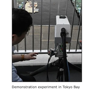
NEC Corporation has developed a technology for measuring sea levels with high accuracy from greater distances using 3D Light Detection And Ranging (LiDAR), a remote sensing technology. This technology makes it possible to reliably measure sea levels, even in the event of a tsunami or ground movement at the location where the measuring equipment is installed. In June 2024, NEC conducted a demonstration test of this technology in Tokyo Bay and confirmed that it can measure sea levels with high accuracy from a greater distance than conventional technologies.
Background
In the event of a tsunami caused by an earthquake, volcanic eruption, or other phenomenon, immediate and accurate assessment of changes in sea levels is critical to saving lives. Current radio wave and float-type sea level measurement systems have a measurement range of about 20 meters from the surface of the sea. However, if ground movement occurs due to an earthquake or other phenomenon, it becomes difficult to measure sea levels. In fact, ground movement due to a major earthquake that occurred on the Noto Peninsula of Japan in January 2024 disabled measurement equipment along part of the coastline, resulting in a delay before reliable measurements could be resumed.
About the New Technology
This new technology delivers 3D-LiDAR infrared laser beams to buoys floating on the sea, and reflected light is used to measure the distance. This ultra-sensitive optical reception is accomplished using long-range 3D-LiDAR with advanced long-range, large-capacity optical transmission and reception technology (coherent reception technology), making it possible to obtain the 3D point cloud data of objects from greater distances. As a result, this is the first time that sea levels have been successfully measured from a distance of 60 meters from the sea with an error of about 2cm. In addition, a 3D water level measurement technology has been developed that clusters processing of the acquired 3D point cloud data, classifies the shape of buoys and surrounding topography with high precision, and then compares the information to correct the position and estimate the height of buoys. This makes it possible to measure from a variety of locations and angles, meaning that 3D-LiDAR equipment can be installed in a wider variety of locations.
3D point cloud data scanned by 3D-LiDAR
As a result, tide stations may be installed in locations along the coastline that are less susceptible to significant ground movement, making the system disaster-resistant and enabling continuous monitoring of sea levels. In addition, the equipment is portable and may be flexibly installed across a wide range of locations, helping to reduce installation costs and time.
Future Developments
Going forward, NEC plans to continue developing this technology, including extending the measurable distance to several hundred meters and improving measurement accuracy by comparing 3D-LiDAR data with map information of the surrounding area, aiming for practical application by the end of FY2025.
Share on:


Suggested Items
SEMI, TechSearch International Release 2025 Edition of Worldwide Semiconductor Assembly & Test Facility Database
07/01/2025 | SEMISEMI and TechSearch International announced the release of the 2025 edition of the Worldwide Semiconductor Assembly & Test Facility Database, the industry’s most comprehensive resource tracking global assembly and test sites operated by integrated device manufacturers (IDMs) and outsourced semiconductor assembly and test providers (OSATs).
IIT Kharagpur Forge Strategic Partnership with Swansea University in Advance Smart Manufacturing and Materials Research
06/18/2025 | IIT KharagpurIn a significant step towards global academic and industrial collaboration, Swansea University and the Indian Institute of Technology Kharagpur (IIT KGP) signed a Memorandum of Understanding (MoU) to deepen research partnerships, promote academic exchange, and foster innovation in advanced manufacturing and materials engineering.
Hon Hai Research Institute Achieves Breakthrough in Quantum Cryptography Recognized by Leading Global Conference
06/17/2025 | FoxconnHon Hai Research Institute (HHRI), the research arm of Hon Hai Technology Group (Foxconn), the world’s largest electronics manufacturer and technology service provider, has achieved a significant breakthrough in quantum computing.
VIAVI, Hanyang University Sign Memorandum of Understanding to Advance 6G Research
06/10/2025 | PRNewswireVIAVI Solutions Inc. and Hanyang University, one of South Korea's leading academic institutions, today announced a Memorandum of Understanding to collaborate on AI-RAN, 5G and 6G research at the university's Beyond-G Global Innovation Center.
Tariff Effects and China Subsidies Soften 1Q25 Downturn; Foundry Revenue Decline Narrows to 5.4%
06/09/2025 | TrendForceTrendForce’s latest investigations find that the global foundry industry recorded 1Q25 revenue of US$36.4 billion—a 5.4% QoQ decline. The downturn was softened by last-minute rush orders from clients ahead of the U.S. reciprocal tariff exemption deadline, as well as continued momentum from China’s 2024 consumer subsidy program.