-

-
News
News Highlights
- Books
Featured Books
- smt007 Magazine
Latest Issues
Current Issue
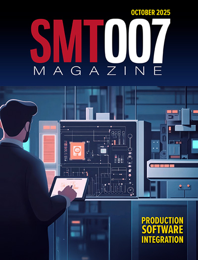
Production Software Integration
EMS companies need advanced software systems to thrive and compete. But these systems require significant effort to integrate and deploy. What is the reality, and how can we make it easier for everyone?

Spotlight on India
We invite you on a virtual tour of India’s thriving ecosystem, guided by the Global Electronics Association’s India office staff, who share their insights into the region’s growth and opportunities.

Supply Chain Strategies
A successful brand is built on strong customer relationships—anchored by a well-orchestrated supply chain at its core. This month, we look at how managing your supply chain directly influences customer perception.
- Articles
- Columns
- Links
- Media kit
||| MENU - smt007 Magazine
Are Domestic Assemblers Ready for the Next Level of Electronics Miniaturization?
February 19, 2025 | Chrys Shea, SHEA Engineering ServicesEstimated reading time: 1 minute
UHDI technology is more than another evolutionary level of miniaturization. It’s a fundamental change in how we create circuit boards, on a scale potentially as impactful as the transition from through-hole to surface mount was 40 years ago.
Traditional and high density interconnect (HDI) PCB manufacturing technology that uses subtractive copper etching processes cannot repeatably produce features below 75 microns and vias below 150 microns. UHDI fabrication blows those limits away with additive or semi-additive processes that can produce lines and spaces as small as 12 microns and vias of 75-100 microns, increasing circuit density by a whopping 10–30X.
UHDI is not new or uncommon technology. It’s in the palm of our hands as it’s been in mobile products since the iPhone 6 launched in 2014. While it has proven its capabilities in consumer electronics, it needs significant development and evaluation to be considered robust enough for aerospace and defense electronics, where the benefits of miniaturization are extensive, but the implication of malfunction is far greater than in similar consumer-grade devices.
As with most modern PCB fabrication technologies, Asia leads America in the development and scaleup of UHDI. To realize the multitude of benefits from PCB densification in security and defense electronics, the U.S. government has begun funding R&D for domestic PCB fabrication, and several shops are gearing up to produce UHDI technology for high-performance, high-reliability applications. While the fabrication industry is abuzz with news of innovative materials, processes, and technologies, the assembly side has remained relatively quiet.
To read the entire article, which published in the February 2025 issue of SMT007 Magazine, click here.
Testimonial
"The I-Connect007 team is outstanding—kind, responsive, and a true marketing partner. Their design team created fresh, eye-catching ads, and their editorial support polished our content to let our brand shine. Thank you all! "
Sweeney Ng - CEE PCBSuggested Items
Episode 6 of Ultra HDI Podcast Series Explores Copper-filled Microvias in Advanced PCB Design and Fabrication
10/15/2025 | I-Connect007I-Connect007 has released Episode 6 of its acclaimed On the Line with... American Standard Circuits: Ultra High Density Interconnect (UHDI) podcast series. In this episode, “Copper Filling of Vias,” host Nolan Johnson once again welcomes John Johnson, Director of Quality and Advanced Technology at American Standard Circuits, for a deep dive into the pros and cons of copper plating microvias—from both the fabricator’s and designer’s perspectives.
Interposers, Substrates, and Advanced Manufacturing
10/13/2025 | Marcy LaRont, I-Connect007I attend a lot of industry trade shows and conferences. Lately, during conversations with technologists, I’ve noticed that there is some confusion about what exactly constitutes an interposer. One question I hear every so often is, “Are all interposers substrates?” The short answer to that question is no. But some interposers are, in fact, full substrates.
I-Connect007 Releases Episode 5 of Groundbreaking Ultra HDI Podcast Series
10/10/2025 | I-Connect007In Episode 5 “Via Structures,” host Nolan Johnson welcomes back John Johnson, Director of Quality and Advanced Technology at American Standard Circuits. Together, they explore the designer’s perspective on UHDI’s impact on via structures, diving into the metallurgy, chemistry, mechanical considerations, and stackup reduction that provide greater design flexibility and fewer constraints than ever before.
New Podcast Episode: How Does UHDI Benefit SWaP?
10/03/2025 | I-Connect007In podcast episode 4, “SWaP Considerations,” host Nolan Johnson welcomes back industry expert John Johnson, Director of Quality and Advanced Technology at American Standard Circuits (ASC). Together, they explore how UHDI delivers measurable advantages in size, weight, and power (SWaP)—unlocking new possibilities in speed, efficiency, and miniaturization.
Connect the Dots: Evolution of PCB Manufacturing—Lamination
10/02/2025 | Matt Stevenson -- Column: Connect the DotsWhen I wrote The Printed Circuit Designer's Guide to...™ Designing for Reality, it was not a one-and-done effort. Technology is advancing rapidly. Designing for the reality of PCB manufacturing will continue to evolve. That’s why I encourage designers to stay on top of the tools and processes used during production, to ensure their designs capitalize on the capabilities of their manufacturing partner.


