


 SMT Perspectives & Prospects: The Architecture of Winston Churchill’s Leadership
 Global Sourcing Spotlight: Making Global Sourcing Simple Again
 The Government Circuit: New Council Now Helps Shape Policy Decisions in the Electronics Supply Chain


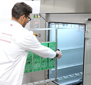
Driving Innovation: Depth Routing Processes—Achieving Unparalleled Precision in Complex PCBs
In PCB manufacturing, the demand for increasingly complex and miniaturized designs continually pushes the boundaries of traditional fabrication methods, including depth routing.
Depth routing is indispensable in several key PCB applications:
- Rigid-flex PCBs: These hybrid boards combine rigid sections with flexible interconnections, requiring precise depth routing for removing the “cup” on top and/or bottom of the flex part.
- PCBs with cavities: Cavities are strategically created within PCB layers to integrate or embed components directly into the board.
- Copper coin PCBs for heat sinks: In high-power applications, copper coins are often embedded within PCBs to serve as highly efficient localized heat sinks. Depth routing is used to create precise pockets for these coins, ensuring a perfect fit.
Success in these applications demands not only on robust machinery but also sophisticated control functions. PCB manufacturers rely on advanced machine features and process methodologies to meet their precise depth routing goals. Here, I’ll explore some crucial functions that empower manufacturers to master complex depth routing challenges.
Depth Routing With a Second Measuring System
A common scenario in depth routing involves creating a constant depth of cut, even when the PCB panel itself is not perfectly flat—a frequent occurrence in manufacturing. In such cases, relying solely on a pre-programmed Z-axis depth from a fixed reference point can lead to inconsistent results.
To overcome this, machines use a second measuring system, typically involving a pressure foot equipped with a specialized insert or brush that precisely touches the surface of the PCB. The machine calculates the depth from the exact moment of contact and maintains it consistently throughout the routing path. This dynamic adjustment ensures that the routed depth is accurate relative to the potentially uneven panel surface. A typical and critical application of this technology is depth routing for cup elimination in rigid-flex PCB manufacturing.
Depth Routing From Electrical Contact
While a second measuring system often uses mechanical contact to establish the initial point for depth calculations, depth routing from electrical contact offers an alternative, precise method that leverages the PCB's electrical properties. In this approach, the layer designated as the starting point for depth calculation must be grounded. This could be the top copper layer or an inner copper layer. The electrically conductive routing tool makes contact with this grounded layer, triggering a precise signal that defines the zero-point for Z-axis depth measurement.
This method is particularly advantageous for applications requiring extremely tight tolerances and direct reference to a conductive layer. It eliminates the minor mechanical variations that can occur with pressure foot systems, offering superior repeatability when the target is a copper feature.
The principles of electrical contact can also be applied in a “polishing” function. This advanced feature ensures an exceptionally clean and precise routed surface, particularly when the depth routing is intended to expose a copper layer without causing damage. The machine executes a depth-routing operation. When the tool makes electrical contact with the target copper layer, the Z-axis movement halts automatically. The tool then advances slightly along the X- and/or Y-axis, lifts minimally in the Z-axis, continues to move in the X and/or Y axes, and subsequently lowers to re-establish electrical contact. This sequence repeats as part of the polishing operation.
This iterative micro-movement ensures that the machine is continuously “feeling” the copper surface. The result is a highly precise depth routing with minimal penetration into the copper, effectively “polishing” the surface by removing any remaining dielectric residue or micro-burrs, leading to a clean copper finish ready for subsequent processes.
Advanced Mapping Possibilities
For applications demanding an equal thickness of the remaining web (the precise distance between the end of the depth routing and the bottom surface of the panel), simple constant depth routing is often insufficient because of inherent variations in panel thickness. In such intricate cases, it’s imperative to create a “map” of the back-up panel (the bottom surface) before the routing process begins.
This mapping involves high-resolution scanning or measurement of the bottom surface topography. The resulting data creates a digital “map” that precisely informs the routing machine about the local thickness variations. The machine's control system then adjusts the Z-axis depth for each routed point according to this map. This ensures that even if the original panel thickness varies, the remaining web thickness is consistently uniform.
Page 1 of 2


