-

- News
- Books
Featured Books
- smt007 Magazine
Latest Issues
Current Issue
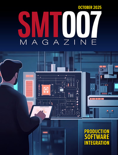
Production Software Integration
EMS companies need advanced software systems to thrive and compete. But these systems require significant effort to integrate and deploy. What is the reality, and how can we make it easier for everyone?

Spotlight on India
We invite you on a virtual tour of India’s thriving ecosystem, guided by the Global Electronics Association’s India office staff, who share their insights into the region’s growth and opportunities.

Supply Chain Strategies
A successful brand is built on strong customer relationships—anchored by a well-orchestrated supply chain at its core. This month, we look at how managing your supply chain directly influences customer perception.
- Articles
- Columns
- Links
- Media kit
||| MENU - smt007 Magazine
Electrodeposited Copper Foils Market to Grow by $11.7 Billion Over 2025-2032
September 18, 2025 | Globe NewswireEstimated reading time: 2 minutes
The global electrodeposited copper foils market is poised for dynamic growth, driven by the rising adoption in advanced electronics and renewable energy storage solutions. Latest industry estimates suggest that the market will reach US$ 13.6 billion by 2025, expanding at a robust CAGR of 9.3% from 2025 to 2032, ultimately achieving a valuation of approximately US$ 25.3 billion by 2032. Key growth drivers include rising investments in high-performance printed circuit boards (PCBs) and the exponential growth of lithium-ion battery (LiB) production for electric vehicles (EVs) and energy storage systems.
Market Insights
With innovations in electronic miniaturization and automotive electrification gaining momentum, there is a heightened demand for ultra-thin and high-performance copper foils. Regulatory emphasis on sustainable energy, particularly in Europe and Asia Pacific, further boosts market expansion, with manufacturers scaling production to meet the demand from EV and energy storage sectors.
Key Drivers
- Expanding EV Battery Production: Global electric mobility trends significantly contribute to the growth of the electrodeposited copper foils industry. As lithium-ion batteries are central to EVs, there is an increasing demand for ultra-thin copper foils as current collectors. Governments' ambitious EV targets prompt manufacturers to innovate thinner, high-performance foils.
- Rising Demand for PCBs in Consumer Electronics: The proliferation of 5G networks and IoT devices heightens the need for advanced PCBs. Electrodeposited copper foils, offering excellent adhesion and uniformity, are critical for manufacturing multilayer PCBs used in smartphones, tablets, laptops, and wearables.
- Technological Advancements in Copper Foil Manufacturing: Continuous R&D enhances foil thickness, surface treatment, and conductivity, presenting new opportunities in flexible PCBs, next-gen batteries, and miniaturized circuits.
Business Opportunities
The market offers lucrative prospects for stakeholders across various sectors. Companies that align with ultra-thin foils for EVs and high-performance foils for PCBs are poised to capture substantial value. The integration of copper foils in renewable energy storage further broadens demand. Partnerships between copper foil manufacturers, EV battery makers, and electronics firms foster innovation, ensuring robust supply chains. Additionally, circular economy initiatives, including copper recycling, present opportunities aligned with sustainability objectives.
Regional Analysis
- Asia Pacific leads the market, anchored by strong EV battery manufacturing in China, South Korea, and Japan. This region benefits from major PCB producers and governmental support for green mobility.
- North America experiences rapid growth, driven by gigafactory expansions in the U.S. and Canada, with a strong EV manufacturer presence.
- Europe's investments in EV battery gigafactories and advanced electronics manufacturing continue to play a crucial role, aligned with stringent environmental policies.
- Latin America and the Middle East & Africa emerge with increasing renewable energy adoption and expanding industrial electronics markets.
Testimonial
"Advertising in PCB007 Magazine has been a great way to showcase our bare board testers to the right audience. The I-Connect007 team makes the process smooth and professional. We’re proud to be featured in such a trusted publication."
Klaus Koziol - atgSuggested Items
Episode 6 of Ultra HDI Podcast Series Explores Copper-filled Microvias in Advanced PCB Design and Fabrication
10/15/2025 | I-Connect007I-Connect007 has released Episode 6 of its acclaimed On the Line with... American Standard Circuits: Ultra High Density Interconnect (UHDI) podcast series. In this episode, “Copper Filling of Vias,” host Nolan Johnson once again welcomes John Johnson, Director of Quality and Advanced Technology at American Standard Circuits, for a deep dive into the pros and cons of copper plating microvias—from both the fabricator’s and designer’s perspectives.
Nolan’s Notes: Tariffs, Technologies, and Optimization
10/01/2025 | Nolan Johnson -- Column: Nolan's NotesLast month, SMT007 Magazine spotlighted India, and boy, did we pick a good time to do so. Tariff and trade news involving India was breaking like a storm surge. The U.S. tariffs shifted India from one of the most favorable trade agreements to the least favorable. Electronics continue to be exempt for the time being, but lest you think that we’re free and clear because we manufacture electronics, steel and aluminum are specifically called out at the 50% tariff levels.
MacDermid Alpha & Graphic PLC Lead UK’s First Horizontal Electroless Copper Installation
09/30/2025 | MacDermid Alpha & Graphic PLCMacDermid Alpha Electronics Solutions, a leading supplier of integrated materials and chemistries to the electronics industry, is proud to support Graphic PLC, a Somacis company, with the installation of the first horizontal electroless copper metallization process in the UK.
MacDermid Alpha Showcases Advanced Interconnect Solutions at PCIM Asia 2025
09/18/2025 | MacDermid Alpha Electronics SolutionsMacDermid Alpha Electronic Solutions, a global leader in materials for power electronics and semiconductor assembly, will showcase its latest interconnect innovations in electronic interconnect materials at PCIM Asia 2025, held from September 24 to 26 at the Shanghai New International Expo Centre, Booth N5-E30
Trouble in Your Tank: Implementing Direct Metallization in Advanced Substrate Packaging
09/15/2025 | Michael Carano -- Column: Trouble in Your TankDirect metallization systems based on conductive graphite are gaining popularity throughout the world. The environmental and productivity gains achievable with this process are outstanding. Direct metallization reduces the costs of compliance, waste treatment, and legal issues related to chemical exposure. A graphite-based direct plate system has been devised to address these needs.


