-
-
News
News Highlights
- Books
Featured Books
- smt007 Magazine
Latest Issues
Current Issue
Spotlight on Mexico
Mexico isn’t just part of the electronics manufacturing conversation—it’s leading it. From growing investments to cross-border collaborations, Mexico is fast becoming the center of electronics in North America. This issue includes bilingual content, with all feature articles available in both English and Spanish.
Production Software Integration
EMS companies need advanced software systems to thrive and compete. But these systems require significant effort to integrate and deploy. What is the reality, and how can we make it easier for everyone?
Spotlight on India
We invite you on a virtual tour of India’s thriving ecosystem, guided by the Global Electronics Association’s India office staff, who share their insights into the region’s growth and opportunities.
- Articles
- Columns
- Links
- Media kit
||| MENU - smt007 Magazine
Now Available—The Companion Guide to… SMT Inspection: Today, Tomorrow, and Beyond: Mastering Metrology for Advanced Semiconductor Packages
October 3, 2025 | I-Connect007Estimated reading time: 1 minute
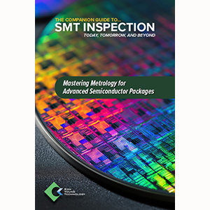
I-Connect007 is pleased to announce the release of an 18-page resource for engineers, technologists, and decision-makers in electronics manufacturing: The Companion Guide to SMT Inspection: Today, Tomorrow, and Beyond: Mastering Metrology for Advanced Semiconductor Packages.
As the industry advances toward increasingly compact and high-performance devices, the demand for precise inspection has never been greater. This downloadable guide explores the pivotal role of metrology in advanced semiconductor packaging, offering expert insights into why True3D inspection is essential, how Koh Young’s advanced metrology platforms are redefining accuracy, and what the future of dimensional measurement holds for technologies such as System-in-Package (SiP), Fan-out Wafer-Level Packaging (FOWLP), and 3D stacked dies.
Key topics covered include:
- The evolution of SMT and semiconductor inspection
- Precision solder and flux inspection with the Meister S and S+
- Die- and component-level analysis with the Meister D and D+
- AI-powered wafer-level metrology with ZenStar
- Flux and underfill inspection with Neptune C+
- Bridging SMT and semiconductor QA with the Zenith series
- Smart factory integration and the future of dimensional metrology
“With advanced packaging driving the next wave of electronics innovation, accurate measurement is the foundation for ensuring connectivity, reliability, and long-term performance,” said author Brent Fischthal. “This guide is designed to help process engineers and manufacturers understand the inspection challenges they face today—and prepare for those just around the corner.”
The Companion Guide to… SMT Inspection: Today, Tomorrow, and Beyond: Mastering Metrology for Advanced Semiconductor Packages is available now as a free download on the I-Connect007 platform.
Testimonial
"The I-Connect007 team is outstanding—kind, responsive, and a true marketing partner. Their design team created fresh, eye-catching ads, and their editorial support polished our content to let our brand shine. Thank you all! "
Sweeney Ng - CEE PCBSuggested Items
Merlin PCB Group Invests in 2 CIMS Galaxy 25µ AOI Machines
11/13/2025 | Merlin PCB GroupThe Merlin PCB group has invested in CIMS Galaxy 25µ AOI machines, one for Merlin Flex in Hartlepool and the other for Merlin Circuit Technology in Hawarden.
GenI Generative AOI Programming Debuts: Mycronic Sets a New Standard in AOI Automation
11/10/2025 | MycronicMycronic’s PCB Assembly Solution division announces the launch of GenI™, an industry first solution designed to liberate electronics manufacturers from the complexities of traditional Automated Optical Inspection (AOI) programming.
Learning With Leo: UHDI—The Next Leap in PCB Manufacturing
11/05/2025 | Leo Lambert -- Column: Learning With LeoHigh density interconnect (HDI) technology has been a cornerstone of miniaturized electronics since Hewlett-Packard introduced the first chip-scale implementation in 1982. Over time, HDI processes became central to organic flip-chip packaging in the semiconductor industry. Today, the convergence of IC substrates and system-level PCBs has accelerated the adoption of UHDI.
Koh Young Technology Appoints Jeff Lee as Head of Industrial Solutions Business
11/03/2025 | Koh Young TechnologyKoh Young Technology, the global leader in True 3D measurement-based inspection and metrology solutions, has appointed Jeff Lee as Head of Industrial Solutions Business.
UHDI Fundamentals: UHDI Technology and Automated Inspection
11/03/2025 | Anaya Vardya, American Standard CircuitsFollowing up on the last article on integrating ultra high density interconnect (UHDI) PCB technologies and Quality 5.0, here we will do a deeper dive into the automated inspection component. UHDI applications demand extreme precision, with line/space dimensions below 25 µm and microvias below 30 µm. Automated inspection systems are essential to achieving the defect-free fabrication required at these scales, and legacy automated inspection systems are becoming obsolete and ineffective.