-
- News
- Books
Featured Books
- design007 Magazine
Latest Issues
Current IssueProper Floor Planning
Floor planning decisions can make or break performance, manufacturability, and timelines. This month’s contributors weigh in with their best practices for proper floor planning and specific strategies to get it right.
Showing Some Constraint
A strong design constraint strategy carefully balances a wide range of electrical and manufacturing trade-offs. This month, we explore the key requirements, common challenges, and best practices behind building an effective constraint strategy.
All About That Route
Most designers favor manual routing, but today's interactive autorouters may be changing designers' minds by allowing users more direct control. In this issue, our expert contributors discuss a variety of manual and autorouting strategies.
- Articles
- Columns
- Links
- Media kit
||| MENU - design007 Magazine
ICD Releases 2015 Version of the ICD Stackup and PDN Planner
July 1, 2015 | In-Circuit Design Pty LtdEstimated reading time: 1 minute

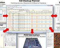
In-Circuit Design Pty Ltd (ICD), Australia, developer of the ICD Stackup and PDN Planner software, has released the 2015 version of their popular software.
Impedance plots have been incorporated into this new release. “The impedance plots are simulated by multiple passes of the field solver (in the background) to create heads-up graphs of how to adjust the particular variables to achieve the target impedance.” said Barry Olney, CEO.
Further, with the addition of Panasonic Megtron 7 E-glass and Low Dk-glass (34MHz) the dielectric materials library has been increased to an impressive 16,700 ready-to-use materials up to 100GHz. There are also over 5,250 capacitors, derived from SPICE models, in the PDN library.
The IPC-2581B format, bi-directional interface has now been thoroughly tested by the IPC-2581 Consortium. “This new feature gives the ICD Stackup Planner the ability to import/export Cadence Allegro 16.6 and OrCAD 16.6 stackups and to import Altium Designer and Zuken CR-8000 & CR-5000 stackups” said Olney.
Existing support customers are advised to contact ICD to obtain download instructions for both the new software and the 2015 license server. Owners of a previous version may upgrade at an affordable price.
About In-Circuit Design Pty Ltd
In-Circuit Design Pty Ltd, based in Australia, developed the ICD Stackup and PDN Planner software, is a PCB Design Service Bureau and specialist in board level simulation. For further information or to download a free evaluation of the software, please go to www.icd.com.au
All trademarks are trademarks of their respective owner.
Testimonial
"Our marketing partnership with I-Connect007 is already delivering. Just a day after our press release went live, we received a direct inquiry about our updated products!"
Rachael Temple - AlltematedSuggested Items
Global PCB Connections: Understanding the General Fabrication Process—A Designer’s Hidden Advantage
08/14/2025 | Markus Voeltz -- Column: Global PCB ConnectionsDesigners don’t need to become fabricators, but understanding the basics of PCB fabrication can save you time, money, and frustration. The more you understand what’s happening on the shop floor, the better you’ll be able to prevent downstream issues. As you move into more advanced designs like HDI, flex circuits, stacked vias, and embedded components, this foundational knowledge becomes even more critical. Remember: the fabricator is your partner.
The Art and Science of PCB Floor Planning: A Comprehensive Guide
08/14/2025 | Cory Grunwald and Jeff Reinhold, Monsoon SolutionsPCB design is an intricate and crucial part of developing electronic products. One of the foundational stages of PCB design is floor planning, a phase where the placement of components and the flow of signals are meticulously mapped out. A good floor plan ensures that the PCB performs well, is easy to manufacture, and meets all mechanical and electrical requirements. We’ll explore the essential aspects of floor planning, from its objectives and process to the challenges that designers face.
EnSilica Establishes New EU Mixed-Signal Design Centre in Budapest, Hungary
08/12/2025 | EnSilicaThe facility strengthens EnSilica’s presence in the European Union and taps into Budapest’s deep technology ecosystem, which hosts numerous leading automotive and industrial multinationals. This expansion will increase the Group’s global headcount to around 210 employees.
Happy’s Tech Talk #41: Sustainability and Circularity for Electronics Manufacturing
08/13/2025 | Happy Holden -- Column: Happy’s Tech TalkI attended INEMI’s June 12 online seminar, “Sustainable Electronics Tech Topic Series: PCBs and Sustainability.” Dr. Maarten Cauwe of imec spoke on “Life Cycle Inventory (LCI) Models for Assessing and Improving the Environmental Impact of PCB Assemblies,” and Jack Herring of Jiva Materials Ltd. spoke on “Transforming Electronics with Recyclable PCB Technology.” This column will review information and provide analysis from both presentations.
Elementary, Mr. Watson: Why Your PCB Looks Like a Studio Apartment
08/13/2025 | John Watson -- Column: Elementary, Mr. WatsonIn November 2022, I wrote a column called "Is Your Bathroom in the Kitchen?" This piece related a bizarre real estate listing that emerged out of St. Louis that had architects scratching their heads and interior designers cringing. Nestled in the historic Central West End sat a 200-square-foot apartment that completely defied logic. It wasn't the size that raised eyebrows, it was the layout. Here's the kicker: While that's rare in real estate, it's shockingly common in PCB design.