


 Fresh PCB Concepts: Engineering Copper Coin and Copper Pedestal Technology With IPC Design Interpretation
 Target Condition: Signal Integrity Without Borders
 Elementary, Mr. Watson: PCB Education in the Midst of the Storms


James Amundson, electronics industry veteran of over 15 years is pleased to announce the launch of Arkeo Stack, an advanced PCB stack-up modeling software, focused on rigid, flex, rigid-flex and IMS PCBs stack-up solutions, targeting design engineers to PCB manufacturers. “Today’s electronics OEM, EMS and PCB companies are challenged in sourcing a cost effective, accurate, intuitive PCB stack-up software that will accommodate, simple to complex interconnect structures and all PCB design types. We believe we have a solution." Amundson Technologies partnered with PCB Companies and industry experts to design a solution to meet and exceed their stack up needs. "We solicited feedback from multiple Front End Engineers, Application Engineers and facility managers, from both rigid and flex PCB manufacturers, in developing Arkeo Stack." Mr. Amundson said.
To list a few of Arkeo stacks features:
- Rigid and Rigid-Flex modeling: Accurately model any number of rigid and flex zones, you can model any build no matter how complex. Accurately model impedance on any section of the build.
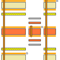
- Complex Interconnect Structures: Accurately model and display; mechanical vs laser vias, filled vs unfilled, stacked vs staggered, and consider copper thickness requirements for copper wrap.
- Accurate and Configurable: Materials are configured to facility thicknesses and specifications, making press thicknesses and impedance very accurate. All aspects of the system are configurable to facility or user needs.
- Impedance Calculations: Impedance calculations are generated using Apsim Rlgc for the most accurate predictions. Includes the ability to model structures with crosshatch reference planes.
- Back Calculation: System will automatically back calculate build dielectric thickness and/or line width given specific impedance requirements.
- Electrical Properties; Automatic calculations of individual layer Dk/Df for more accurate impedance predictions.
- Easy to use interface: The interface is very intuitive and easy to use, allowing users to master the software without a long learning curve.
- BOM generation: Bill of Materials with panel specific costs can be generated to view or input into most quotation packages.
- Customizable Reports: Reports are fully customizable allowing you to use your company's logo and display in the format of your choice. Multiple reports can be configured allowing users to have the output they need. Reports can be printed or saved directly to Pdf.
- Panelization: Built-in panelization layout tool. Layout panels with individual boards or arrays, add coupons, rails, etc. Arrays can be layed-out by fixed array size or by a matrix of boards. Full dimensions can be added to the array.
- "Industry feedback has been extremely positive." Amundson continued, "A Tier One OEM benchmarked our product against existing software systems in 2014. The results from their engineering staff gave Arkeo Stack the best report. We now have multiple installations in the US and Canada."
More information on Arkeo Stack can be found at www.arkeostack.com.


