-

- News
- Books
Featured Books
- smt007 Magazine
Latest Issues
Current Issue
What's Your Sweet Spot?
Are you in a niche that’s growing or shrinking? Is it time to reassess and refocus? We spotlight companies thriving by redefining or reinforcing their niche. What are their insights?

Moving Forward With Confidence
In this issue, we focus on sales and quoting, workforce training, new IPC leadership in the U.S. and Canada, the effects of tariffs, CFX standards, and much more—all designed to provide perspective as you move through the cloud bank of today's shifting economic market.

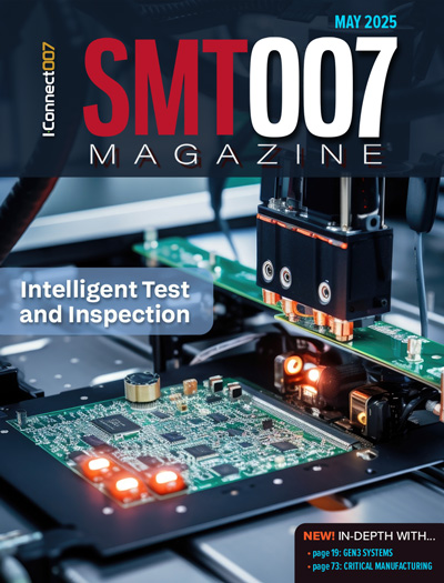
Intelligent Test and Inspection
Are you ready to explore the cutting-edge advancements shaping the electronics manufacturing industry? The May 2025 issue of SMT007 Magazine is packed with insights, innovations, and expert perspectives that you won’t want to miss.
- Articles
- Columns
- Links
- Media kit
||| MENU - smt007 Magazine
ZESTRON’s Ravi Parthasarathy to Present at IMAPS’s Advances in Semiconductor Packaging Exhibition
September 21, 2015 | ZESTRONEstimated reading time: 1 minute
ZESTRON, the globally leading provider of high precision cleaning products, services and training solutions in the electronics manufacturing and semiconductor industries, is pleased to announce that Ravi Parthasarathy, Senior Process Engineer, ZESTRON, will present “Impact of Cleaning Technologies on Lead Frame Packages: The Difference in Wire Bond Yields” at IMAPS’s Advances in Semiconductor Packaging Exhibition on September 24th.
Leadframe packages are widely used for semiconductor device fabrication. Typically, the interconnections between an integrated circuit (IC) and the metal leads are made through the process of die attach and wire bonding. For die attach processes, the standard materials used are epoxy, adhesive or solder paste. Prior to wire bonding and molding processes, it is critical to remove post-solder flux residues in order to maximize overall yield. For companies that are manufacturing semiconductor devices, it is common to produce millions of units per day. As a result, incremental improvement in wire bond yield by a fraction of a percent can significantly impact production efficiency and the final product cost model.
This presentation reviews a design of experiment that was developed to improve a semicon manufacturer’s cleaning process and the resulting wire bond yield.
IMAPS’s Advances in Semiconductor Packaging will be held at SUNY Polytechnic Institute on Thursday, September 24th from 8:00 AM to 5:00 PM. For more information on ZESTRON’s product lines, services, and learning opportunities, please visit our booth.
About ZESTRON
Headquartered in Manassas, Virginia, and operating in more than 35 countries, ZESTRON is the globally leading provider of high precision cleaning products, services and training solutions for the electronics manufacturing industry. With six worldwide technical centers and the largest team of chemical engineers in the industry, ZESTRON’s commitment to ensuring that its customers surpass even the most stringent cleaning requirements is without equal.
Suggested Items
Driving Innovation: Direct Imaging vs. Conventional Exposure
07/01/2025 | Simon Khesin -- Column: Driving InnovationMy first camera used Kodak film. I even experimented with developing photos in the bathroom, though I usually dropped the film off at a Kodak center and received the prints two weeks later, only to discover that some images were out of focus or poorly framed. Today, every smartphone contains a high-quality camera capable of producing stunning images instantly.
Hands-On Demos Now Available for Apollo Seiko’s EF and AF Selective Soldering Lines
06/30/2025 | Apollo SeikoApollo Seiko, a leading innovator in soldering technology, is excited to spotlight its expanded lineup of EF and AF Series Selective Soldering Systems, now available for live demonstrations in its newly dedicated demo room.
Indium Corporation Expert to Present on Automotive and Industrial Solder Bonding Solutions at Global Electronics Association Workshop
06/26/2025 | IndiumIndium Corporation Principal Engineer, Advanced Materials, Andy Mackie, Ph.D., MSc, will deliver a technical presentation on innovative solder bonding solutions for automotive and industrial applications at the Global Electronics A
Fresh PCB Concepts: Assembly Challenges with Micro Components and Standard Solder Mask Practices
06/26/2025 | Team NCAB -- Column: Fresh PCB ConceptsMicro components have redefined what is possible in PCB design. With package sizes like 01005 and 0201 becoming more common in high-density layouts, designers are now expected to pack more performance into smaller spaces than ever before. While these advancements support miniaturization and functionality, they introduce new assembly challenges, particularly with traditional solder mask and legend application processes.
Knocking Down the Bone Pile: Tin Whisker Mitigation in Aerospace Applications, Part 3
06/25/2025 | Nash Bell -- Column: Knocking Down the Bone PileTin whiskers are slender, hair-like metallic growths that can develop on the surface of tin-plated electronic components. Typically measuring a few micrometers in diameter and growing several millimeters in length, they form through an electrochemical process influenced by environmental factors such as temperature variations, mechanical or compressive stress, and the aging of solder alloys.


