


 Nolan’s Notes: Finding Your Sweet Spot
 Standard of Excellence: Delivering Excellence—A Daily Goal
 Knocking Down the Bone Pile: Tin Whisker Mitigation in Aerospace Applications, Part 3


Kester to Present at the 12th Annual IWLPC and Tabletop Exhibition
October 5, 2015 | KesterEstimated reading time: 1 minute
Kester will present at the 12th Annual International Wafer-Level Packaging Conference and Tabletop Exhibition which takes place October 13-15 at the DoubleTree San Jose Airport Hotel, San Jose, California.
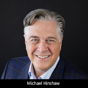
On October 14 at 10:45AM, Dan Duffy, Research Scientist, will present “Assemblies Containing Copper Pillar Structures Processed Using One Step Chip Attach Materials (OSCA) and Conventional Mass Reflow Processing”.
To learn more about Kester’s product offering and capabilities, please visit our website at www.kester.com
Speaker Biography
Daniel J. Duffy, PhD, is currently working at Kester Inc. as a Technology Development Manager and Research Scientist with a focus on developing of materials for semiconductor assembly materials and electronic packaging. He received a Ph.D. in Chemistry with research focus on physical chemistry/polymer physics and also holds a B.S. in Chemical Engineering. Both degrees were received from the University of Massachusetts at Amherst. Industrial research experience includes 8+ years focused on developing filler/particle dispersion, surface modification technology, complex fluid rheology design for industrial adhesive applications and high performance electronic packaging and assembly adhesives. Additional areas of research experience include thermodynamic/kinetic aspects of phase behavior in multi component reactive polymer blends, computational chemical modeling, molecular transport kinetics in thin polymer films, photo polymerization, molecular interactions in imprinted polymer films, diamond film coating, and spectroscopic characterization of polymers. Dan is an inventor on 5 patents and has authored over 15 publications in the fields of physical chemistry, polymers, composites and electronic assembly materials.
About Kester
Kester is a global supplier of assembly materials for the Electronic Assembly and Semiconductor Packaging industries. Kester is focused on delivering innovative, robust and high-quality solutions to help our customers address their technological challenges. Kester’s current product portfolio includes soldering attachment materials such as solder paste, soldering chemicals, TSF (tacky solder flux) materials, and metal products such as bar, solid and flux-cored wire. Kester is an Illinois Tool Works (ITW) company. ITW is a Fortune 200 company that produces engineered fasteners and components, equipment and consumable systems, and specialty products. It employs approximately 49,000 people, and is based in Glenview, Illinois, with operations in 57 countries.
Share on:


Suggested Items
Driving Innovation: Direct Imaging vs. Conventional Exposure
07/01/2025 | Simon Khesin -- Column: Driving InnovationMy first camera used Kodak film. I even experimented with developing photos in the bathroom, though I usually dropped the film off at a Kodak center and received the prints two weeks later, only to discover that some images were out of focus or poorly framed. Today, every smartphone contains a high-quality camera capable of producing stunning images instantly.
Hands-On Demos Now Available for Apollo Seiko’s EF and AF Selective Soldering Lines
06/30/2025 | Apollo SeikoApollo Seiko, a leading innovator in soldering technology, is excited to spotlight its expanded lineup of EF and AF Series Selective Soldering Systems, now available for live demonstrations in its newly dedicated demo room.
Indium Corporation Expert to Present on Automotive and Industrial Solder Bonding Solutions at Global Electronics Association Workshop
06/26/2025 | IndiumIndium Corporation Principal Engineer, Advanced Materials, Andy Mackie, Ph.D., MSc, will deliver a technical presentation on innovative solder bonding solutions for automotive and industrial applications at the Global Electronics A
Fresh PCB Concepts: Assembly Challenges with Micro Components and Standard Solder Mask Practices
06/26/2025 | Team NCAB -- Column: Fresh PCB ConceptsMicro components have redefined what is possible in PCB design. With package sizes like 01005 and 0201 becoming more common in high-density layouts, designers are now expected to pack more performance into smaller spaces than ever before. While these advancements support miniaturization and functionality, they introduce new assembly challenges, particularly with traditional solder mask and legend application processes.
Knocking Down the Bone Pile: Tin Whisker Mitigation in Aerospace Applications, Part 3
06/25/2025 | Nash Bell -- Column: Knocking Down the Bone PileTin whiskers are slender, hair-like metallic growths that can develop on the surface of tin-plated electronic components. Typically measuring a few micrometers in diameter and growing several millimeters in length, they form through an electrochemical process influenced by environmental factors such as temperature variations, mechanical or compressive stress, and the aging of solder alloys.