


 Nolan’s Notes: Finding Your Sweet Spot
 Standard of Excellence: Delivering Excellence—A Daily Goal
 Knocking Down the Bone Pile: Tin Whisker Mitigation in Aerospace Applications, Part 3


Photo Stencil Presents at IWLPC 2015
October 8, 2015 | Photo Stencil, LLCEstimated reading time: 1 minute
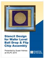
Photo Stencil, LLC, a leading full-service provider of high-performance stencils and tooling, announces that Susan Holmes, VP engineering and customer service for Photo Stencil, will present the paper Stencil Design for Wafer Level Ball Drop and Flip Chip Assembly at the IWLPC during Session 10 on Wednesday, October 14, 2015, at 5:00 PM. The 12th Annual International Wafer-Level Packaging Conference and Tabletop Exhibition is being held at the Doubletree San Jose Airport Hotel, San Jose, CA.
Stencils are now being used for wafer bumping, wafer level ball placement, and mixed assembly of flip chip and SMT. The presentation will describe new methods of stencil printing, the types of stencils, configurations, and performance.
"Stencil design -- aperture size, stencil thickness, the stencil material, the smoothness of the apertures, spacing between apertures, and area ratio -- plays a major role in maximizing performance," explained Holmes. "The use of stencils is no longer confined to just the PCB industry or laser formed stencils. They now contribute significantly to the semiconductor assembly process and are made of new materials, in cleanrooms, and often using laser direct imaging."
For more information, contact Photo Stencil at info@photostencil.com, call 719-599-4305, or check out the website at www.photostencil.com.
About Photo Stencil
Photo Stencil, LLC provides high-performance stencils, squeegee blades, thick film and metal mask screens and tooling for the surface mount technology (SMT) assembly, solar, and semiconductor industries. Its innovations include the patented AMTX E-FAB® electroform stencils, high-performance, proprietary NicAlloy™, NicAlloy-XT™, laser-cut, and chemetch stencils, and patented electroformed E-Blade® squeegee blade. Stencil design support and customer-specific design libraries are also provided. Founded in 1979, Photo Stencil is headquartered in Colorado Springs and has a manufacturing facility in Mexico.
Share on:


Suggested Items
Facing the Future: Time for Real Talk, Early and Often, Between Design and Fabrication
07/08/2025 | Prashant Patel -- Column: Facing the FutureThere has always been a subtle but significant divide between those who design and those who build printed circuit boards. It’s not a hostile gap, but it is a real one, and in today’s high-speed, high-complexity, high-stakes environment, that gap is costing us more than time and yield. It’s costing us innovation.
DownStream Acquisition Fits Siemens’ ‘Left-Shift’ Model
06/26/2025 | Andy Shaughnessy, I-Connect007I recently spoke to DownStream Technologies founder Joe Clark about the company’s acquisition by Siemens. We were later joined by A.J. Incorvaia, Siemens’ senior VP of electronic board systems. Joe discussed how he, Rick Almeida, and Ken Tepper launched the company in the months after 9/11 and how the acquisition came about. A.J. provides some background on the acquisition and explains why the companies’ tools are complementary.
Elementary Mr. Watson: Retro Routers vs. Modern Boards—The Silent Struggle on Your Screen
06/26/2025 | John Watson -- Column: Elementary, Mr. WatsonThere's a story about a young woman preparing a holiday ham. Before putting it in the pan, she cuts off the ends. When asked why, she shrugs and says, "That's how my mom always did it." She asks her mother, who gives the same answer. Eventually, the question reaches Grandma, who laughs and says, "Oh, I only cut the ends off because my pan was too small." This story is a powerful analogy for how many PCB designers approach routing today.
Connect the Dots: The Future of PCB Design and Manufacturing
07/02/2025 | Matt Stevenson -- Column: Connect the DotsFor some time, I have been discussing the increasing complexity of PCBs and how designers can address the constantly evolving design requirements associated with them. My book, "The Printed Circuit Designer’s Guide to… Designing for Reality," details best practices for creating manufacturable boards in a modern production environment.
Siemens Turbocharges Semiconductor and PCB Design Portfolio with Generative and Agentic AI
06/24/2025 | SiemensAt the 2025 Design Automation Conference, Siemens Digital Industries Software today unveiled its AI-enhanced toolset for the EDA design flow.