


 Target Condition: Signal Integrity Without Borders
 Elementary, Mr. Watson: PCB Education in the Midst of the Storms
 Beyond Design: How Signals Survive the Hostile PCB Environment


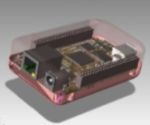
Mentor Graphics Corporation today announced new PADS 3D tool capabilities plus major usability enhancements to the PADS flow for printed circuit board (PCB) design. The new technology provides visualization, placement, and design rule checking in 3D, minimizing iterations with mechanical and manufacturing teams. Schematic design and layout enhancements improve usability across the flow for increased user productivity.
"The photorealistic PADS 3D tool (with solder mask turned ON) made it very clear, very quickly that I had a problem. Without it, we would have had to document/disposition the issue, correct the design, ECO the release documents/drawings … not to mention take a reputation hit with the customer," stated Robert Berrington, electrical engineer, DornerWorks, Ltd. "With PADS, we were able to find and correct the error before it left the building!"
New PADS 3D Capabilities
The powerful 3D engine within the PADS product enables full 3D visualization, placement, design rule checking and PDF creation. The commercial engine also provides faster and more robust performance compared to traditional open-source software, supporting large databases with ease. PADS tool users can import STEP [Standard for The Exchange of Product Data] models, as well as export full PCB assemblies in multiple formats. This release also extends the 3D functionality in the PADS Professional product with an optional four million parts 3D library and ECAD-MCAD collaboration tool. 3D capabilities are scalable depending on the PADS product configuration.
Front-to-Back Usability Improvements
The latest PADS product release includes many enhancements to improve the user experience and increase productivity. The PADS layout has been updated to include enhanced reference designator placement with physical design reuse elements, improved padstack editing, and updated translator and migration tools. The PADS schematic capture feature now includes the ability to automatically renumber a schematic sheet and update the bill of materials (BOM) report.
Design starts can be accelerated with a new sample library, and access to the Mentor component portal, now populated with schematic symbols, footprints, and parametric data for over 450K parts. Translators from competitive tools have been updated, including import of Altium® V15 libraries and designs.
"PADS is a market-leading PCB design solution and we are addressing the needs of our customers with this new release," stated Paul Musto, PADS product line director, Mentor Graphics Systems Design Division. "This demonstrates Mentor's continued commitment and investment in PADS by providing our customers with easy-to-use, feature-rich technologies so they get to market faster with highest-quality products."
About Mentor Graphics
Mentor Graphics Corporation is a world leader in electronic hardware and software design solutions, providing products, consulting services and award-winning support for the world's most successful electronic, semiconductor and systems companies. Established in 1981, the company reported revenues in excess of $1.24 billion. Corporate headquarters are located at 8005 S.W. Boeckman Road, Wilsonville, Oregon 97070-7777.


