-

- News
- Books
Featured Books
- smt007 Magazine
Latest Issues
Current Issue
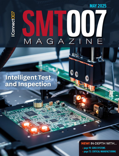
Intelligent Test and Inspection
Are you ready to explore the cutting-edge advancements shaping the electronics manufacturing industry? The May 2025 issue of SMT007 Magazine is packed with insights, innovations, and expert perspectives that you won’t want to miss.

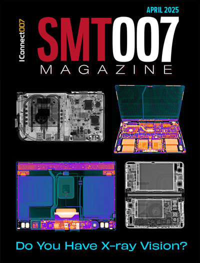
Do You Have X-ray Vision?
Has X-ray’s time finally come in electronics manufacturing? Join us in this issue of SMT007 Magazine, where we answer this question and others to bring more efficiency to your bottom line.

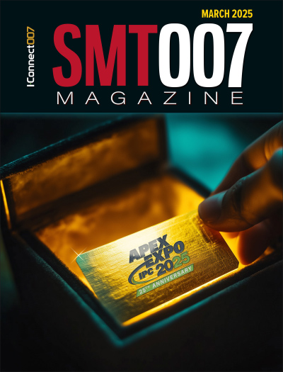
IPC APEX EXPO 2025: A Preview
It’s that time again. If you’re going to Anaheim for IPC APEX EXPO 2025, we’ll see you there. In the meantime, consider this issue of SMT007 Magazine to be your golden ticket to planning the show.
- Articles
- Columns
Search Console
- Links
- Media kit
||| MENU - smt007 Magazine
Alpha Talks Challenges of Solder Recycling
December 22, 2015 | Patty Goldman, I-Connect007Estimated reading time: 13 minutes
Fullerton: Absolutely. In fact, less than a month ago, I had a customer call me and request our most current version of the declarations for conflict minerals and the source of our materials. We have a pretty robust environmental compliance and health and safety group that are also involved in ensuring that we do take materials from safe areas—not from areas that would be illegal or immoral to take materials from. We have all of the declarations ready for our customers. They can go right online and download immediately if they want. They’ll get an instant email for the most current version. Once they register, they will automatically get a copy of any future revision as soon as it's released.
Goldman: That's got to be really good for them.
Fullerton: It's good for everyone. It's good for the world. We have to take care of the world that we live in, right?
Goldman: Yes we do. What else is going on with you and your part in Alpha?
Fullerton: It's a busy time in the industry because everything is getting really small. That tends to challenge the manufacturing processes. The smaller things get, the more difficult they are to manufacture. The more difficult things are to manufacture and process, the more our customers need involvement from tech support, like myself and my colleagues at Alpha.
It's one of the things we pride ourselves on is providing excellent research and development, and a high level of technical support to our customers. We're not just selling them materials. We're also selling them the ability to use those materials, perhaps even better than they understand how to. By hiring people that are from a very strong background in processing from the industry, it can unveil things to the customers.
Goldman: Now, you make solder paste, I've been reading some articles about nanoparticles and very fine solder paste, things for the very fine features, right?
Fullerton: Yes. The smaller the feature, generally the smaller the powder you want to use in the solder paste.
Goldman: How does that come about? Talk about that a little bit.
Fullerton: The manufacturing process for that is pretty interesting. I don't fully understand it because I'm not manufacturing the material, but we are making smaller powders now than ever before. We're putting more and more research into smaller and smaller particle size materials. Here's a good example. Ten years ago, we developed our first commercially available lead-free solder paste. It was developed with Type 3 materials. That was the most common materials.
Goldman: Type 3 means what? It has to do with the particle size?
Fullerton: The particle diameter of 80% of the particles is between 25 and 45 microns. There's a specification on what Type 3 can entail. Seven or eight years ago when we made the second generation materials, we developed that as a Type 4 material. Our research and development uses a Type 4 material for all the testing that goes on. Then we made a Type 3 version of that. It showed how the market could shift in that short amount of time.
Goldman: Type 4 is what particle size?
Fullerton: That's where 90% of the particles’ diameters are between 20 and 38 microns. It's a slight shift smaller, but it changed the way we design and develop materials. Our R&D focused on the Type 4 version of that product because we saw that was going to be the most common type that we sold. Nowadays, it really is one of the most common types that we sell for new applications, that new product that we at developed that time. We have another new product coming out shortly. It's been released in Asia. We're scaling up in North America. It is our first product that's developed using a Type 5 powder size, which is where 90% of particles are between 15—25 microns in diameter. You can see the development of the materials is working towards smaller and smaller particle sizes. Now this material will be available in the Type 4, but the smaller the particle size, the more challenging it is to develop a flux package that works really well with that.
Goldman: That was the other thing, because you need more flux that with the smaller particles?
Fullerton: In these, more activity. There's more for the flux to do. The flux has more work to do with smaller particle sizes. It has to do with the fact that for every unit of volume, there's more surface area of powder in the smaller particle size paste, as compared to the same volume of a larger particle size paste. That large of a surface area requires more protection and treatment from the flux during the soldering process. So there's more for it to do when you're actually soldering. It's more challenging. As we go down in particle size, it has also challenged our chemists to develop materials that are appropriate for those smaller particle sizes.
Goldman: They jet solder also?
Fullerton: Yes. There's equipment out there that can jet a small deposit of solder paste. For those pieces of equipment, the smaller the particle size, the smaller the minimum feature size they can jet. The dot size becomes small. They can use and work on smaller designs. That's one area where the market pressure to get smaller and smaller particles is coming from, the people who are jetting.
Goldman: Now, when you have solder paste, there is no dross?
Fullerton: Correct. There's no dross from that process.
Goldman: Your recycling is really for the wave solder applications?
Fullerton: Well, there is some waste out of the SMT process. There's always going to be a little bit of residue left in the container—the jar, the tube, etc. There are wipes and tools and things like that as well. As a service for the customers that engage us for recycling, we'll also recycle their scrap. We can reclaim very small amounts of metals from this. It's not really something we make a lot of money on. We offer it as a service for those currently engaging in our recycling services. We do it as a service for the user so we're kind of a one-stop shop. We can also certify that the scrap and the waste material and the wipes and those sorts of materials were also recycled properly so that none of the metal content goes back into the environment.
Goldman: Seems like a real win-win.
Fullerton: Especially for people still using tin-lead solders; those materials are generally considered hazardous. The way to dispose of them has to be treated much differently than a non-hazardous material. If you sell it to us or ship it to us, and we reclaim it, it's not being put back into environment. It's being put back into other solders. It's a much more environmentally friendly way of dealing with waste than to send it to a landfill.
Goldman: As an aside, is there much call for tin-lead solders anymore?
Fullerton: There is—the high reliability industries, aerospace and military. The medical industry is losing some of their exemptions soon, but right now they're still pretty much a tin-lead industry. For products that are sold only domestically there are still a number of customers that are making products that, if they were sold in the EU, would have to be lead-free. Because they only sell to the North America market, they're using old fashioned tin-lead solder paste. They're still out there.
Page 2 of 3
Suggested Items
Indium’s Karthik Vijay to Present on Dual Alloy Solder Paste Systems at SMTA’s Electronics in Harsh Environments Conference
05/06/2025 | Indium CorporationIndium Corporation Technical Manager, Europe, Africa, and the Middle East Karthik Vijay will deliver a technical presentation on dual alloy solder paste systems at SMTA’s Electronics in Harsh Environments Conference, May 20-22 in Amsterdam, Netherlands.
SolderKing Achieves the Prestigious King’s Award for Enterprise in International Trade
05/06/2025 | SolderKingSolderKing Assembly Materials Ltd, a leading British manufacturer of high-performance soldering materials and consumables, has been honoured with a King’s Award for Enterprise, one of the UK’s most respected business honours.
Knocking Down the Bone Pile: Gold Mitigation for Class 2 Electronics
05/07/2025 | Nash Bell -- Column: Knocking Down the Bone PileIn electronic assemblies, the integrity of connections between components is paramount for ensuring reliability and performance. Gold embrittlement and dissolution are two critical phenomena that can compromise this integrity. Gold embrittlement occurs when gold diffuses into solder joints or alloys, resulting in mechanical brittleness and an increased susceptibility to cracking. Conversely, gold dissolution involves the melting away of gold into solder or metal matrices, potentially altering the electrical and mechanical properties of the joint.
'Chill Out' with TopLine’s President Martin Hart to Discuss Cold Electronics at SPWG 2025
05/02/2025 | TopLineBraided Solder Columns can withstand the rigors of deep space cold and cryogenic environments, and represent a robust new solution to challenges facing next generation large packages in electronics assembly.
BEST Inc. Reports Record Demand for EZReball BGA Reballing Process
05/01/2025 | BEST Inc.BEST Inc., a leader in electronic component services, is pleased to announce they are experiencing record demand for their EZReball™ BGA reballing process which greatly simplifies the reballing of ball grid array (BGA) and chip scale package (CSP) devices.


