













 The Marketing Minute: Marketing Is a Team Sport
 The Right Approach: Old Philosophies, New Tools
 Trouble in Your Tank: HDI and UHDI—Building the Foundation of Advanced Packaging





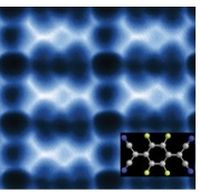
In what could prove to be a significant advance in the fabrication of graphene-based nanodevices, a team of Berkeley Lab researchers has discovered a new mechanism for assembling two-dimensional (2D) molecular “islands” that could be used to modify graphene at the nanometer scale. These 2D islands are comprised of F4TCNQ molecules that trap electrical charge in ways that are potentially useful for graphene-based electronics.
“We’re reporting a scanning tunneling microscopy and non-contact atomic force microscopy study of F4TCNQ molecules at the surface of graphene in which the molecules coalesce into 2D close-packed islands,” says Michael Crommie, a physicist who holds joint appointments with Berkeley Lab’s Materials Sciences Division and UC Berkeley’s Physics Department. “The resulting islands could be used to control the charge-carrier density in graphene substrates, as well as to modify how electrons move through graphene-based devices. They might also be used to form precise nanoscale patterns that exhibit atomic-scale structural perfection unmatched by conventional fabrication techniques.”
Crommie is one of four corresponding authors of a paper describing this research published by ACS Nano. The paper is titled “Molecular Self-Assembly in a Poorly Screened Environment: F4TCNQ on Graphene/BN.” The other corresponding authors are Steven Louie and Marvin Cohen, both with Berkeley Lab and UC Berkeley, and Jiong Lu of the National University of Singapore.
Graphene is a sheet of pure carbon just one atom thick through which electrons speed 100 times faster than they move through silicon. Graphene is also slimmer and stronger than silicon, making it a potential superstar material for the electronics industry. However, graphene must be electrically doped to tune the number of charge carriers it contains in order to be useful in devices, and F4TCNQ has proven to be an effective dopant for transforming graphene into a “p-type” semiconductor.
“F4TCNQ is known to extract electrons from a substrate, thus changing the substrate charge-carrier density,” Crommie says. “Previous studies looked at F4TCNQ adsorbed on graphene supported by a metal substrate, which creates a highly screened environment. F4TCNQ adsorbed on graphene supported by the insulator boron nitride (BN) creates a poorly screened environment. We found that, unlike with metals, F4TCNQ molecules on graphene/BN form 2D islands by a unique self-assembly mechanism that is driven by the long-range Coulomb interactions between the charged molecules. Negatively-charged molecules coalesce into an island, increasing the local work function above the island and causing additional electrons to flow into the island. These additional electrons cause the total energy of the graphene layer to decrease, resulting in island cohesion.”
Page 1 of 2


