


 Dan’s Biz Bookshelf: Four Important Books You Need to Read (Not Just Say You Have)
 The Marketing Minute: Cracking the Code of Technical Marketing


Zooming Around a Photonic Chip
March 18, 2016 | Joint Quantum InstituteEstimated reading time: 5 minutes
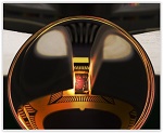
When it comes to quantum physics, light and matter are not so different. Under certain circumstances, negatively charged electrons can fall into a coordinated dance that allows them to carry a current through a material laced with imperfections. That motion, which can only occur if electrons are confined to a two-dimensional plane, arises due to a phenomenon known as the quantum Hall effect.
Researchers, led by Mohammad Hafezi, a JQI Fellow and assistant professor in the Department of Electrical and Computer Engineering at the University of Maryland, have made the first direct measurement that characterizes this exotic physics in a photonic platform. The research was published online Feb. 22 and featured on the cover of the March 2016 issue of Nature Photonics. These techniques may be extended to more complex systems, such as one in which strong interactions and long-range quantum correlations play a role.
Symmetry and Topology
Physicists use different approaches to classify matter; symmetry is one powerful method. For instance, the microscopic structure of a material like diamond looks the same even while shifting your gaze to a new spot in the crystal. These symmetries – the rotations and translations that leave the microscopic structure the same – predict many of the physical properties of crystals.
Symmetry can actually offer a kind of protection against disruptions. Here, the word protection means that the system (e.g. a quantum state) is robust against changes that do not break the symmetry. Recently, another classification scheme based on topology has gained significant attention. Topology is a property that depends on the global arrangement of particles that make up a system rather than their microscopic details. The excitement surrounding this mathematical concept has been driven by the idea that the topology of a system can offer a stability bubble around interesting and even exotic physics, beyond that of symmetry. Physicists are interested in harnessing states protected by both symmetry and topology because quantum devices must be robust against disturbances that can interfere with their functionality.
The quantum Hall effect is best understood by peering through the lens of topology. In the 1980s, physicists discovered that electrons in some materials behave strangely when subjected to large magnetic fields at extreme cryogenic temperatures. Remarkably, the electrons at the boundary of the material will flow along avenues of travel called ‘edge states’, protected against defects that are most certainly present in the material. Moreover, the conductance--a measure of the current--is quantized. This means that when the magnetic field is ramped up, then the conductance does not change smoothly. Instead it stays flat, like a plateau, and then suddenly jumps to a new value. The plateaus occur at precise values that are independent of many of the material’s properties. This hopping behavior is a form of precise quantization and is what gives the quantum Hall effect its great utility, allowing it to provide the modern standard for calibrating resistance in electronics, for instance.
Researchers have engineered quantum Hall behavior in other platforms besides the solid-state realm in which it was originally discovered. Signatures of such physics have been spotted in ultracold atomic gases and photonics, where light travels in fabricated chips. Hafezi and colleagues have led the charge in the photonics field.
Page 1 of 2
Share on:


Testimonial
"The I-Connect007 team is outstanding—kind, responsive, and a true marketing partner. Their design team created fresh, eye-catching ads, and their editorial support polished our content to let our brand shine. Thank you all! "
Sweeney Ng - CEE PCBSuggested Items
Rules of Thumb: Design007 Magazine, November 2024
11/11/2024 | I-Connect007 Editorial TeamRules of thumb are everywhere, but there may be hundreds of rules of thumb for PCB design. They’re built on design formulas, fabricators’ limitations, and tribal knowledge. And unfortunately, some longtime rules of thumb should be avoided at all costs. How do we separate the wheat from the chaff, so to speak?
Connect the Dots: Best Practices for Prototyping
09/21/2023 | Matt Stevenson -- Column: Connect the DotsPCB prototyping is a critical juncture during an electronic device’s journey from concept to reality. Regardless of a project’s complexity, the process of transforming a design into a working board is often enlightening in terms of how a design can be improved before a PCB is ready for full production.
The Drive Toward UHDI and Substrates
09/20/2023 | I-Connect007 Editorial TeamPanasonic’s Darren Hitchcock spoke with the I-Connect007 Editorial Team on the complexities of moving toward ultra HDI manufacturing. As we learn in this conversation, the number of shifting constraints relative to traditional PCB fabrication is quite large and can sometimes conflict with each other.
Asia/Pacific AI Spending Surge to Reach a Projected $78 Billion by 2027
09/19/2023 | IDCAsia/Pacific spending on Artificial Intelligence (AI) ), including software, services, and hardware for AI-centric systems will grow to $78.4 billion in 2027, according to International Data Corporation's latest Worldwide Artificial Intelligence Spending Guide.
Intel to Sell Minority Stake in IMS Nanofabrication Business to TSMC
09/13/2023 | IntelIntel Corporation announced that it has agreed to sell an approximately 10% stake in the IMS Nanofabrication business to TSMC. TSMC’s investment values IMS at approximately $4.3 billion, consistent with the valuation of the recent stake sale to Bain Capital Special Situations.