















 Dan’s Biz Bookshelf: ‘Building a Story Brand 2.0’
 It’s Only Common Sense: Why Should They Take Your Call?





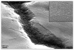
The secret to a long-hidden magic trick behind the self-assembly of nanocrystal structures is starting to be revealed.
The transformation of simple colloidal particles — bits of matter suspended in solution — into tightly packed, beautiful lace-like meshes, or superlattices, has puzzled researchers for decades. Pretty pictures in themselves, these tiny superlattices, also called quantum dots, are being used to create more vivid display screens as well as arrays of optical sensory devices. The ultimate potential of quantum dots to make any surface into a smart screen or energy source hinges, in part, on understanding how they form.
Through a combination of techniques including controlled solvent evaporation and synchrotron X-ray scattering, the real time self-assembly of nanocrystal structures has now become observable in-situ. The findings were reported in the journal Nature Materials in a paper by Assistant Professor William A. Tisdale and grad student Mark C. Weidman, both at MIT’s Department of Chemical Engineering, and Detlef-M. Smilgies at the Cornell High Energy Synchrotron Source (CHESS).
The researchers anticipate their new findings will have implications for the direct manipulation of resulting superlattices, with the possibility of on-demand fabrication and the potential to generate principles for the formation of related soft materials such as proteins and polymers.
Quantum dot disco
Tisdale and his colleagues are among the many groups who study hard semiconductor nanocrystals with surfaces coated with organic molecules. These solution-processable electronic materials are on store shelves now under a variety of names, incorporated into everything from lighting displays to TVs. They also are being eyed for making efficient solar cells and other energy conversion devices due to their ease of fabrication and low-cost manufacturing processes.
The broader adoption of these nanocrystals into other energy conversion technologies has been limited, in part, by the lack of knowledge about how they self-assemble, going from colloidal particles (like tiny Styrofoam balls suspended in a liquid) to superlattices (picture those same balls now dry, packed, and aligned).
Techniques including electron microscopy and dynamic light scattering have uncovered some aspects of the starting colloidal state and the final superlattice structure, but they have not illuminated the transition between these two states. In fact, such foundational work dates back to the mid-1990s with Moungi Bawendi’s group at MIT.
“In the past 10 to 15 years, a lot of progress has been made in making very beautiful nanocrystal structures,” Tisdale says. “However, there’s still a lot of debate about why they assemble into each configuration. Is it ligand entropy or the faceting of the nanocrystals? The depth of information provided by watching the entire self-organization process unfold in real time can help answer these questions.”
Page 1 of 2
Share on:



Subscribe
Stay ahead of the technologies shaping the future of electronics with our latest newsletter, Advanced Electronics Packaging Digest. Get expert insights on advanced packaging, materials, and system-level innovation, delivered straight to your inbox.
Subscribe now to stay informed, competitive, and connected.
Suggested Items
ASC Sunstone Circuits to Exhibit and Present Lunch-and-Learn at PCB West 2026
09/21/2026 | ASC Sunstone CircuitsASC Sunstone Circuits will exhibit at PCB West 2026, taking place September 29 through October 2 at the Santa Clara Convention Center in Santa Clara, California. The PCB West exhibition will be held Wednesday, September 30.
Indium Promotes Chris Bastecki to Business Unit Vice President
09/11/2026 | Indium CorporationIndium Corporation is pleased to announce the promotion of Chris Bastecki to Business Unit Vice President, Americas Sales & Service and Global Printed Circuit Board (PCB) Assembly Materials Marketing.
RapidDirect Launches PCB Division to Integrate PCB and Mechanical Manufacturing
09/11/2026 | Globe NewswireRapidDirect, a leading global provider of custom on-demand digital manufacturing, announced the official launch of its new Printed Circuit Board (PCB) division.
Heller and SEHO Investing in Mexico
09/09/2026 | Nolan Johnson, SMT007 MagazineHeller Industries is the leading provider of thermal systems in the electronics assembly and semiconductor industries, manufacturing a wide range of equipment, primarily for standard reflow applications in electronics assembly. The company has realized significant business growth in Mexico in recent years and is now preparing for SMTA Guadalajara. Paul Lancaster, vice president of sales and marketing, spoke about the Mexican market, growing a local support infrastructure, and partnering with SEHO.
Indium to Explore the Critical Materials and Packaging Process Connection at CPRIM 2026
09/01/2026 | Indium CorporationIndium Corporation® Senior Area Technical Manager Luis Pan will discuss how precisely matching materials and assembly processes can positively impact yield and reliability at the Conference on Advanced Packaging Reliability Technology and Interconnect Materials (CPRIM) 2026, September 4, in Guangzhou, China.