


 Dan’s Biz Bookshelf: Four Important Books You Need to Read (Not Just Say You Have)
 The Marketing Minute: Cracking the Code of Technical Marketing


Magnetic Field Affects Electrons During Etching
March 31, 2016 | University of TokyoEstimated reading time: 1 minute
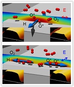
A Japanese and French international research group, using surface polishing employing light with a controlled direction of oscillation, has for the first time demonstrated that a magnetic field with extremely high frequency (in the petahertz rage. One petahertz corresponds to one trillion oscillation per second) can be used for nanofabrication.
The technology to create nanoscale flat surfaces is essential for the development of electronic devices and optical devices. However, conventional chemical and mechanical polishing methods damage the surface and leave behind impurities. To solve this problem, a University of Tokyo research group developed a non-contact light-based polishing technique called near-field etching that is capable of eliminating surface unevenness. However, it was thought that it was the electric field, not the magnetic field, which contributed to the polishing effect in near-field etching.
The research group of Associate Professor Takashi Yatsui at the University of Tokyo Graduate School of Engineering and Associate Professor Katsuyuki Nobusada at the Institute for Molecular Science and their colleagues examined surface irregularities of zirconia (ZrO2, a transparent material with a high refractive index also known as a type of imitation diamond) during the near-field etching process, and found that the magnetic field determined the properties of the etching process rather than the electric field.
“This discovery revealed that magnetic field oscillating with light frequency can be utilized for fabrication. Although light is an oscillating electric and magnetic field, a magnetic field oscillating with the frequency of visible light does not have any effect on materials. Thus, the effect of the magnetic field was ignored and only the effect of the electric field was considered for applications in light-based fabrication,” explains Yatsui. He continues, “Therefore this is a very surprising result that is in contradiction with what is considered common knowledge. We hope that this discovery will contribute not only to basic research but also to the fabrication of nanostructures for advanced optical and electrical devices.”
Share on:


Testimonial
"In a year when every marketing dollar mattered, I chose to keep I-Connect007 in our 2025 plan. Their commitment to high-quality, insightful content aligns with Koh Young’s values and helps readers navigate a changing industry. "
Brent Fischthal - Koh YoungSuggested Items
Driving Innovation: Depth Routing Processes—Achieving Unparalleled Precision in Complex PCBs
09/08/2025 | Kurt Palmer -- Column: Driving InnovationIn PCB manufacturing, the demand for increasingly complex and miniaturized designs continually pushes the boundaries of traditional fabrication methods, including depth routing. Success in these applications demands not only on robust machinery but also sophisticated control functions. PCB manufacturers rely on advanced machine features and process methodologies to meet their precise depth routing goals. Here, I’ll explore some crucial functions that empower manufacturers to master complex depth routing challenges.
Polar Instruments Announces Additive Transmission Line Support for Si9000e
08/20/2025 | Polar InstrumentsTransmission lines embedded into the PCB surface are a feature of UHDI constructions. The 2025 fall release of Polar's Si9000e PCB impedance & insertion loss transmission line field solver incorporates eight new single ended, differential and coplanar transmission line structures.
Henniker Plasma Launches Stratus Turnkey Plasma Manufacturing Cell
08/13/2025 | Henniker PlasmaHenniker Plasma, a leading manufacturer of plasma treatment systems, proudly announces the launch of its Stratus Plasma Manufacturing Cell range — a fully integrated, turnkey solution that combines advanced atmospheric plasma surface treatment with robotic automation.
Trouble in Your Tank: Metallizing Flexible Circuit Materials—Mitigating Deposit Stress
08/04/2025 | Michael Carano -- Column: Trouble in Your TankMetallizing materials, such as polyimide used for flexible circuitry and high-reliability multilayer printed wiring boards, provide a significant challenge for process engineers. Conventional electroless copper systems often require pre-treatments with hazardous chemicals or have a small process window to achieve uniform coverage without blistering. It all boils down to enhancing the adhesion of the thin film of electroless copper to these smooth surfaces.
Designers Notebook: Basic PCB Planning Criteria—Establishing Design Constraints
07/22/2025 | Vern Solberg -- Column: Designer's NotebookPrinted circuit board development flows more smoothly when all critical issues are predefined and understood from the start. As a basic planning strategy, the designer must first consider the product performance criteria, then determine the specific industry standards or specifications that the product must meet. Planning also includes a review of all significant issues that may affect the product’s manufacture, performance, reliability, overall quality, and safety.