


 Nolan’s Notes: Is Mexico the Pulse of Electronics in the Americas?
 Standard of Excellence: Speed vs. Quality in Customer Service
 Knocking Down the Bone Pile: Revamp Your Components with BGA Reballing


Selective Soldering: Design, Process Challenges and Practical Solutions
April 28, 2016 | Pete Starkey, I-Connect007Estimated reading time: 8 minutes
Although SMT is today’s predominant electronics assembly technology and the proportion of through-hole components continues to decline, the need for some through-hole assembly will remain for many years. As component density and board complexity increase, hand-soldering can no longer be relied upon to give acceptable or repeatable results and selective soldering techniques are growing in popularity. What is the most reliable and cost effective solution to through hole soldering in tin-lead and lead-free environments? What are the design and process challenges and what are the practical solutions?
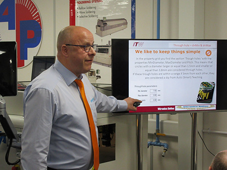
A SMART Group workshop at the Bromsgrove, UK, premises of equipment and process materials distributor APP Electronics, set out to provide the answers, with a programme combining technical presentations, live demonstrations and hands-on sessions, introduced and moderated by Nigel Burtt, senior electronics manufacturing engineer at Renishaw and SMART Technical Committee Chairman.
Burtt launched the proceedings with a general overview of selective soldering processes, focusing on multi-point dip-nozzle soldering and single point mini-wave nozzle soldering, and described two main classes of machine, where either a robot brought the PCB assembly to a stationary soldering nozzle, or the nozzle moved to a stationary PCB assembly on a conveyor, showing examples of each type.
In principle, the objective was to mimic wave-soldering, but in localised areas. Flux was applied selectively to specific component leads, the PCB was pre-heated to drive off solvents and activate the flux, and then the component leads were brought into contact with the solder wave. A continuous flow of nitrogen around the solder nozzle was essential in selective soldering, to keep the nozzle free from dross, and could be used as a means of additional local pre-heating. The type and size of soldering nozzle was chosen to suit components and PCBs. Single point mini-wave nozzles could be used for dip soldering single leads or drag soldering multiple leads; smaller sizes gave less heat transfer and larger sizes enabled higher speeds. Burtt showed a series of video illustrations of various actual soldering operations.
Solder pot temperatures were generally higher than would be used in wave soldering, placing more constraints on the performance of the flux and potentially more local thermal stress on components and PCB materials. Additionally, there was a greater tendency for copper to be dissolved from component leads and PCB pads, especially with lead-free alloys, and Burtt recommended reference to the Good Practice Guide MAT 26, available free-of-charge on the NPL website. Layout design rules needed to take into account the additional clearances required to accommodate selective soldering, and it was recommended to remove solder mask between pads to eliminate solder balls.
Success in selective soldering is critically dependent on choosing a suitable flux, and placing it exactly where it is required. This was the essence of the first of two presentations from Wim Schouten, regional sales manager for Vitronics Soltec. He explained that although a strong flux was required to clean oxidised metal surfaces and support wetting, there were potential risks to reliability if the right formulation was not chosen.
He advised against using the same flux as used for regular wave soldering because the conditions were significantly different: in a wave soldering application all of the flux came into contact with liquid solder, the high temperature of which de-activated the flux chemistry. In selective soldering not all flux made contact with solder, and residual activators could cause reliability problems. Reliability considerations aside, selective soldering temperatures tended to be significantly higher than in regular wave soldering, so the flux might not be strong enough to work effectively and result in soldering defects. Furthermore, wave soldering flux formulations contained surfactants to promote spreading to cover the complete solder side of the PCB. In selective soldering, excessive spreading of was undesirable although the flux needed to be capable of penetrating the barrels of plated-through holes. Alcohol-based fluxes were preferred to water-based formulations because rapid solvent evaporation resulted in less spreading and higher flux solids per unit area.Page 1 of 3
Share on:


Testimonial
"Advertising in PCB007 Magazine has been a great way to showcase our bare board testers to the right audience. The I-Connect007 team makes the process smooth and professional. We’re proud to be featured in such a trusted publication."
Klaus Koziol - atgSuggested Items
BTU International Earns 2025 Step-by-Step Excellence Award for Its Aqua Scrub™ Flux Management System
10/29/2025 | BTU International, Inc.BTU International, Inc., a leading supplier of advanced thermal processing equipment for the electronics manufacturing market, has been recognized with a 2025 Step-by-Step Excellence Award (SbSEA) for its Aqua Scrub™ Flux Management Technology, featured on the company’s Pyramax™ and Aurora™ reflow ovens.
On the Line With… Ultra HDI Podcast—Episode 7: “Solder Mask: Beyond the Traces,” Now Available
10/31/2025 | I-Connect007I-Connect007 is excited to announce the release of the seventh episode of its 12-part podcast series, On the Line With… American Standard Circuits: Ultra HDI. In this episode, “Solder Mask: Beyond the Traces,” host Nolan Johnson sits down with John Johnson, Director of Quality and Advanced Technology at American Standard Circuits, to explore the essential role that solder mask plays in the Ultra HDI (UHDI) manufacturing process.
Rehm Wins Mexico Technology Award for CondensoXLine with Formic Acid
10/17/2025 | Rehm Thermal SystemsModern electronics manufacturing requires technologies with high reliability. By using formic acid in convection, condensation, and contact soldering, Rehm Thermal Systems’ equipment ensures reliable, void-free solder joints — even when using flux-free solder pastes.
Indium Experts to Deliver Technical Presentations at SMTA International
10/14/2025 | Indium CorporationAs one of the leading materials providers to the power electronics assembly industry, Indium Corporation experts will share their technical insight on a wide range of innovative solder solutions at SMTA International (SMTAI), to be held October 19-23 in Rosemont, Illinois.
Knocking Down the Bone Pile: Revamp Your Components with BGA Reballing
10/14/2025 | Nash Bell -- Column: Knocking Down the Bone PileBall grid array (BGA) components evolved from pin grid array (PGA) devices, carrying over many of the same electrical benefits while introducing a more compact and efficient interconnect format. Instead of discrete leads, BGAs rely on solder balls on the underside of the package to connect to the PCB. In some advanced designs, solder balls are on both the PCB and the BGA package. In stacked configurations, such as package-on-package (PoP), these solder balls also interconnect multiple packages, enabling higher functionality in a smaller footprint.