


 Trouble in Your Tank: Causes of Plating Voids, Pre-electroless Copper
 Dan’s Biz Bookshelf: ‘Growth Hacker Marketing’
 Happy’s Tech Talk #38: Novel Metallization for UHDI


Copper Laminates Made From Transparent Polyimide Films Now Available
August 26, 2016 | DKN ResearchEstimated reading time: 3 minutes
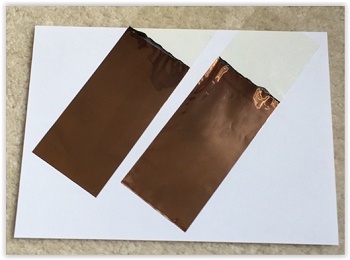
Significant progress has been made over the last few years in building transparent and heat resistant flexible circuits. Several transparent materials were developed along with special manufacturing processes. A copper laminate made from a thin transparent polyimide file plated with a copper layer on both sides for use in traditional manufacturing processes is now available. DKN Research developed a new copper metalizing process using transparent polyimide films. The new laminate will provide manufacturing capabilities using transparent flexible circuits for traditional printed circuit manufacturers.
Polyimide films are the primary substrate material for heat resistant flexible circuits because of the balanced performances between heat resistance and physical properties. The problem is they tend to have an orange or brown color, so the film’s transparency is very low. This is a huge barrier for any optical applications. PET films are another popular substrate material for transparent flexible circuits, but their heat resistance is too low and will not work in standard assembling processes such as soldering and wire bonding. A couple of new heat resistant resins such as LCP have been synthesized and are considered the next generation material for flexible circuits; however, they may not be transparent either. Many chemists used to question the availability of a product that is both transparent and heat resistant. That has changed. Several chemists were successful in synthesizing transparent polyimide resins, and a few companies have brought to market some thin transparent polyimide films that serve as the substrate for heat-resistant flexible circuits.
There are still a few technical hurdles in building transparent flexible circuits. The biggest one is the availability of an appropriate copper laminate for the standard photolithography/chemical etching process. Some of the copper laminates had problems with the surface treatment and gluing of the copper. The transparency of the circuits was remarkably reduced by absorption and scattering.
DKN Research developed a total solutions package for transparent flexible circuits based on each application. During the R&D process, DKN Research has established an electroless and electroplating process of nickel, copper and gold on the transparent polyimide films that provides thin copper laminates available for the standard photolithography/etching process of high density flexible circuits. The new copper laminate could be valuable for traditional flexible circuit manufacturers, because the new laminate does not need any additional equipment or chemicals to build transparent flexible circuits. The transparency of the circuits can be over 85%.
The standard construction of the laminate uses double-sided 3-micron thick copper layers on a 25-micron thick transparent polyimide film. The copper thickness can be thinner at 0.2 microns, and wider thickness ranges will be available for circuit manufacturers. The thin copper conductor could be valuable for semi-additive processes for ultra-fine flexible circuits with microvia holes in the transparent flexible circuits. DKN Research will provide free laminate samples along with a processing guide to circuit manufacturers.
DKN Research will upgrade the laminates and process capabilities to build the leading edge flexible circuits. DKN Research is happy to share the materials and information with circuit manufacturers and device manufacturers. Click here to view a short clip about their products and services.
About DKN Research
DKN Research is a global engineering leader for microelectronics and packaging, specializing in printable & flexible electronics. DKN Research has developed a broad range of leading edge technologies from materials to final devices based on customers’ requirements. They are capable of managing many kinds of materials and manufacturing processes to build and create new devices based on customer needs.
DKN Research provides a broad range of engineering and consulting services not only for the manufacturing community but also the R&D and quality assurance professionals. DKN Research welcomes all inquiries to assist in creating your own circuit devices using its broad range of processing technologies.
Share on:


Suggested Items
RF PCB Design Tips and Tricks
05/08/2025 | Cherie Litson, EPTAC MIT CID/CID+There are many great books, videos, and information online about designing PCBs for RF circuits. A few of my favorite RF sources are Hans Rosenberg, Stephen Chavez, and Rick Hartley, but there are many more. These PCB design engineers have a very good perspective on what it takes to take an RF design from schematic concept to PCB layout.
Trouble in Your Tank: Causes of Plating Voids, Pre-electroless Copper
05/09/2025 | Michael Carano -- Column: Trouble in Your TankIn the business of printed circuit fabrication, yield-reducing and costly defects can easily catch even the most seasoned engineers and production personnel off guard. In this month’s column, I’ll investigate copper plating voids with their genesis in the pre-plating process steps.
Elephantech: For a Greener Tomorrow
04/16/2025 | Marcy LaRont, PCB007 MagazineNobuhiko Okamoto is the global sales and marketing manager for Elephantech Inc., a Japanese startup with a vision to make electronics more sustainable. The company is developing a metal inkjet technology that can print directly on the substrate and then give it a copper thickness by plating. In this interview, he discusses this novel technology's environmental advantages, as well as its potential benefits for the PCB manufacturing and semiconductor packaging segments.
Trouble in Your Tank: Organic Addition Agents in Electrolytic Copper Plating
04/15/2025 | Michael Carano -- Column: Trouble in Your TankThere are numerous factors at play in the science of electroplating or, as most often called, electrolytic plating. One critical element is the use of organic addition agents and their role in copper plating. The function and use of these chemical compounds will be explored in more detail.
IDTechEx Highlights Recyclable Materials for PCBs
04/10/2025 | IDTechExConventional printed circuit board (PCB) manufacturing is wasteful, harmful to the environment and energy intensive. This can be mitigated by the implementation of new recyclable materials and technologies, which have the potential to revolutionize electronics manufacturing.