


 It’s Only Common Sense: More Great Business Ideas from ‘Breaking Bad’
 Material Insight: The Dielectric Constant of PCB Materials
 American Made Advocacy: What About the Rest of the Technology Stack?
Graphene Key to Two-dimensional Semiconductor with Extraordinary Properties
August 30, 2016 | Pennsylvania State UniversityEstimated reading time: 3 minutes
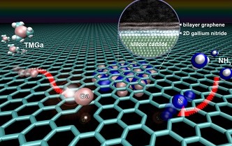
A newly discovered method for making two-dimensional materials could lead to new and extraordinary properties, particularly in a class of materials called nitrides, say the Penn State materials scientists who discovered the process. This first-ever growth of two-dimensional gallium nitride using graphene encapsulation could lead to applications in deep ultraviolet lasers, next-generation electronics and sensors.
"These experimental results open up new avenues of research in 2D materials," says Joshua Robinson, associate professor of materials science and engineering. "This work focuses on making 2D gallium nitride, which has never been done before."
Gallium nitride in its three-dimensional form is known to be a wide-bandgap semiconductor. Wide-bandgap semiconductors are important for high frequency, high power applications. When grown in its two-dimensional form, gallium nitride transforms from a wide-bandgap material to an ultrawide-bandgap material, effectively tripling the energy spectrum it can operate in, including the whole ultraviolet, visible and infrared spectrum. This work will have a particular impact on electro-optic devices that manipulate and transmit light.
"This is a new way of thinking about synthesizing 2D materials," said Zak Al Balushi, a Ph.D. candidate coadvised by Robinson and Joan Redwing, professor of materials science and engineering and electrical engineering. Al Balushi is lead author on a paper appearing online today (Aug.29) in the journal Nature Materials titled "Two-Dimensional Gallium Nitride Realized via Graphene Encapsulation."
"We have this palette of naturally occurring 2D materials," he continued. "But to expand beyond this, we have to synthesize materials that do not exist in nature. Typically, new material systems are highly unstable. But our growth method, called Migration Enhanced Encapsulated Growth (MEEG), uses a layer of graphene to assist the growth and stabilize a robust structure of 2D gallium nitride."
The graphene is grown on a substrate of silicon carbide, which is a technologically important substrate used widely in industry for LEDs, radar and telecommunications. When heated, the silicon on the surface decomposes and leaves a carbon-rich surface that can reconstruct into graphene. The advantage of producing the graphene in this way is that the interface where the two materials meet is perfectly smooth.
Robinson believes that in the case of two-dimensional gallium nitride, the addition of a layer of graphene makes all the difference. Graphene, a one-atom-thick layer of carbon atoms, is known for its remarkable electronic properties and strength.
"It's the key," Robinson says. "If you try to grow these materials the traditional way, on silicon carbide, you normally just form islands. It doesn't grow in nice layers on the silicon carbide."
When gallium atoms are added to the mix, they migrate through the graphene and form the middle layer of a sandwich, with graphene floating on top. When nitrogen atoms are added, a chemical reaction takes place that turns the gallium and nitrogen into gallium nitride.
"The MEEG process not only produces ultra-thin sheets of gallium nitride but also changes the crystal structure of the material, which may lead to entirely new applications in electronics and optoelectronics," said Redwing.
Additional coauthors include Ke Wang, Rafael Vila, Sarah Eichfield, Yu-Chuan Lin and Shruti Subramanian of Penn State, Ram Krishna Ghosh and Suman Datta of Notre Dame, Joshua Caldwell, U.S. Naval Research Laboratory, Xiaoye Qin and Robert Wallace The University of Texas at Dallas and Dennis Paul, Physical Electronics USA.
The Asahi Glass Co., Ltd, Japan, and the U.S. National Science Foundation provided funding for this project. The NSF Materials Science and Engineering Center at Penn State provided funding for Al Balushi. Other funding was provided by the Alfred P. Sloan Foundation, the Penn State Materials Characterization Laboratory and the Center for Low Energy Systems Technology (LEAST), funded by the Semiconductor Research Corporation and DARPA.
Share on:


Suggested Items
Material Insight: The Dielectric Constant of PCB Materials
05/17/2024 | Dr. Preeya Kuray -- Column: Material InsightIn the world of PCB design, miniaturization can be achieved by using low dielectric constant (Dk) materials. Low Dk materials can allow for a reduction in thickness while maintaining a given trace width, leading to lower transmission loss and higher density circuitry.
IPC APEX EXPO: Some Thoughts About Growth
05/16/2024 | Dan Feinberg, I-Connect007After two and a half days of wandering the aisles at IPC APEX EXPO 2024, for the first time, I almost felt like I was exploring CES. There were so many booths and exhibits that I could describe, but I’d like to focus on the growth and huge value of this event, which has expanded well beyond just the growing and impressive exhibit show floor.
The Shaughnessy Report: Unlock Your High-speed Material Constraints
05/15/2024 | Andy Shaughnessy -- Column: The Shaughnessy ReportThe world of PCB materials used to be a fairly simple one. It was divided into two groups: the “traditional” laminates, often called FR-4, and the high-speed laminates developed especially for high-speed PCBs. These were two worlds that usually didn’t collide. But then traditional laminates started getting better, and high-speed designers and design engineers took notice and started to reconsider what FR-4 could be used for.
Breaking High-speed Material Constraints: Design007 Magazine — May 2024
05/14/2024 | I-Connect007 Editorial TeamDo you need specialty materials for your high-speed designs? Maybe not. Improvements in resins mean designers of high-speed boards can sometimes use traditional laminate systems instead of high-speed materials, saving time and money while streamlining the fab process. In the May 2024 issue of Design007 Magazine, our contributors explain how to avoid overconstraining your materials when working with high-speed boards.
Indium Experts to Present at Electronics in Harsh Environments SMTA Conference
05/13/2024 | Indium Corporationndium Corporation Technical Manager for Europe, Africa, and the Middle East, Karthik Vijay, will deliver a technical presentation and Indium Corporation Senior Technologist, Dr. Ronald Lasky, will deliver both a workshop and technical presentation at the Electronics in Harsh Environments SMTA Conference on May 14-16 in Copenhagen, Denmark.