


 It’s Only Common Sense: Marketing Isn’t Fluff, It’s Ammunition
 Driving Innovation: Mechanical and Optical Processes During Rigid-flex Production
 The Chemical Connection: Onshoring PCB Production—Daunting but Certainly Possible


Splitting Hairs: The Manufacture of HDI and Substrate Test Fixtures
May 14, 2015 | Todd Kolmodin, Gardien ServicesEstimated reading time: 2 minutes
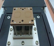
Testing of higher-density product has become ever more challenging with the advancement of chip technology. BGAs, CCDs and other active components have decreased in size so much that historical industry accepted test methodology can no longer effectively test these newer substrates incorporating this higher technology.
Universal grid test machines in North America, for the most part, are limited to single and double-density grids. Dedicated (wired) fixtures can combat some of the density issues faced in today’s test arena, but to successfully succeed in the high-volume demand market a test solution must be found to efficiently test the product and also provide automation to reduce cost.
Universal multi-plate fixtures routinely use test pins down to .3 mm. As pin size decreases, the need for extra plates in the fixture increases, so as to stabilize the pin and provide accurate loading of the pin. However, critical mass is soon reached as the fixture can no longer be solved due to inadequate grid contact availability. Further, as the density is maximized the fixture loses internal support and finally becomes unstable producing false defects, excessive troubleshooting and lost time.
Additionally, there is an ever-increasing demand for 4WK measurement especially on HDI boards, requiring two probes contacting the same pad simultaneously, which can only be tackled, especially for volume production, with this or similar technology.
HDI Fixtures vs. Substrate Fixtures
Quad and octal density universal equipment is used for standard HDI fixturing. Pin sizes for this type of fixturing are usually 90–110μm with a length of 20–30mm, therefore much smaller and shorter than standard universal grid fixtures.
To put this in to perspective the human hair has an average diameter of about 70μm (micron.) Pins in a substrate fixture of current generation typically are 70–50μm; the next generation under development will reach 40–25μm.
Substrate fixtures are typically not used with universal test machines. They require a much higher grid density; therefore the grid itself is generated as a wired solution either to standard connectors or to a universal one-touch interface depending on the final machine used.
HDI fixture usually test a complete test array, whereas substrate fixtures usually test only one or two images of the entire array and the machine will step the board through in multiple tests. That is mainly done to achieve the high accuracy required to test those kinds of boards and the extreme cost and time involved to make these fixture.
HDI fixture typically can be produced within 48 hours, the manufacturing time for a substrate fixture is usually 100–200 hours, and extreme cases can even take longer.
The manufacturing process for the substrate fixture is much more complex than the standard universal fixture. Accuracy is absolutely critical for the success of registering the product to the fixture.
There are basically six steps in the manufacturing process whether it is a hybrid design or a tension probe design:
1. DFM—Engineering
2. Drill
3. Electrode level—wiring, electroplating
4. Probe level—adding probes (wires)
5. Final assembly
6. Final QC and test setup
Editor's Note: This article originally appeared in the April issue of The PCB Magazine.
Share on:


Testimonial
"In a year when every marketing dollar mattered, I chose to keep I-Connect007 in our 2025 plan. Their commitment to high-quality, insightful content aligns with Koh Young’s values and helps readers navigate a changing industry. "
Brent Fischthal - Koh YoungSuggested Items
TTCI Brings Hands-On Test Engineering and IPC Training Expertise to PCB Carolina 2025
10/31/2025 | The Test Connection Inc.The Test Connection Inc. (TTCI), a trusted provider of electronic test and manufacturing solutions, and The Training Connection LLC (TTC-LLC) will exhibit at PCB Carolina on Wednesday, November 12, 2025, at the McKimmon Center at NC State University in Raleigh, North Carolina. Attendees can visit Table 4 to say hello to Bert Horner and Bill Graver, and learn more about their test engineering services and technical training programs.
GEN3 Systems to Showcase Advanced Reliability Test Solutions at productronica 2025 in Munich
10/29/2025 | Gen3 SystemsGEN3 a leader in innovative reliability test solutions, is excited to announce its participation at productronica 2025, the world’s premier trade fair for electronics development and production.
Unlocking the Promise of AI in Electronics Manufacturing
10/29/2025 | Shobhit Agrawal, Keysight TechnologiesThe electronics manufacturing industry is rapidly evolving as more complicated products are introduced in the production lines, which require technological advancements even in the production processes. The requirements for production that is efficient, product quality that is greater, and product life cycles that are shorter are more crucial than ever before. In the electronic device life cycle, from design to maintenance, test phases have a significant impact on the economy of the company. Test processes are closely linked to the production volume and impacted by the complexity of the product. For businesses to maintain their competitive edge, they need to adopt innovative solutions and redefine processes.
New Episode of Voices of the Industry Podcast Explores Breakthroughs in Test and Inspection
10/22/2025 | I-Connect007In this episode of Voices of the Industry, “Testing Innovation: Advances in Test, Inspection & Failure Analysis,” host Nolan Johnson speaks with Rob Boguski, president of Datest. Together, they explore the expanding world of circuit testing, inspection, and failure analysis, areas that are experiencing a surge in technological capability and sophistication. As Johnson and Boguski discuss, today’s test companies are performing analyses and precision methods that would have seemed impossible just a decade ago.
HT Global Circuits Adds Two atg Luther & Maelzer Flying Probe Test Systems
10/15/2025 | atg Luther & Maelzer GmbHAtg Luther & Maelzer GmbH, a leading supplier of electrical testing solutions for the PCB industry, and IEC USA, a distributor of consumables, equipment, and services in the North American PCB market, confirm the order for high-speed bare board testing technology.