


 Standard of Excellence: Building Excellence From the Inside Out
 Powering the Future: Why True Ceramic Circuits Are Not Just ‘Better PCBs’
 Global Sourcing Spotlight: The Global Quality Gap—Why Consistency Wins the Contract


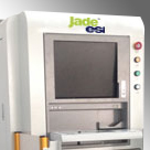
Electro Scientific Industries, Inc., an innovator of laser-based manufacturing solutions for the micromachining industry, today introduced Jade™, the new low-cost, high-volume-production laser micromachining platform adaptable to a range of configurations for different applications including cutting, marking, drilling and engraving.
The new platform addresses challenges faced by manufacturers in the fast-changing consumer electronics segment where they cope with new materials, new technologies and evolving consumer expectations. Meanwhile, there is relentless pressure to reduce costs, meet quality requirements and achieve high-volume high-yield production. The Jade™ platform is the first laser micromachining platform capable of meeting all these diverse requirements, offering unprecedented levels of versatility and cost-efficient operation.
"Production requirements in consumer electronics are constantly changing with new materials and features that require a range of laser micromachining processes that can be delivered quickly and at an attractive cost of ownership," said Edward C. Grady, President and CEO of ESI. "We are directly addressing this challenge with the Jade™ platform. Designed by ESI's cooperative China-USA engineering operation, this low-cost platform is adaptable, reliable, and locally built and serviced by our support teams on the ground in China."
The Jade™ platform is designed to provide contract and consumer electronics manufacturers with a smarter manufacturing option through the use of extendable and configurable stages, lasers, and automation. The base platform can be configured with multiple laser and optics options as well as a range of add-on options including pre- and post-inspection, metrology and advanced alignment automation. All configurations use a common user interface to reduce training time.
This flexibility means that a Jade™ platform can address multiple marking, cutting, and drilling applications in a responsive and cost-effective manner, improving the useful lifespan of the tool and significantly lowering overall cost of ownership for our customers. The Jade™ platform continues ESI's commitment to reliability, responsive local support in China, and to meeting expectations for precision and high-volume yields.
Availability
The Jade™ Series of platforms are available now in China, Vietnam, India, Korea and Taiwan. For more information go to www.esi.com.
About ESI
ESI's integrated solutions allow industrial designers and process engineers to control the power of laser light to transform materials in ways that differentiate their consumer electronics, wearable devices, semiconductor circuits and high-precision components for market advantage. ESI's laser-based manufacturing solutions feature the micro-machining industry's highest precision and speed, and target the lowest total cost of ownership. ESI is headquartered in Portland, Ore., with global operations from the Pacific Northwest to the Pacific Rim. More information is available at www.esi.com.


