


 The Marketing Minute: Marketing With Layers
 The Right Approach: Electro-Tek—A Williams Family Legacy, Part 1
 It’s Only Common Sense: If You’re Not Differentiated, You’re Dead


Ucamco Launches 3 Wavelength Series of Ledia Direct Imaging Systems
September 24, 2015 | UcamcoEstimated reading time: 3 minutes
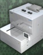
Ucamco is delighted to announce the new 3 Wavelength series of Ledia Direct Imaging (DI) systems for the accurate, high-speed exposure of the industry's most demanding soldermask, inner-layer and outer-layer resists.
When it comes to the direct imaging of PCB materials, Dai Nippon Screen's Ledia multi-wavelength UV LED DI platform has always led the field. First, with its 2 Wavelength Ledia imaging systems, Screen delivered unprecedented DI throughputs on even the most demanding inner- and outer-layer resists, and it gave PCB manufacturers the very first DI technology with which to process standard soldermask resists accurately and at production speeds.
Now, building on that success, Ucamco is launching Screen's 3 Wavelength series. These 5 and 6 exposure head systems combine optimised 365, 385 and 405nm wavelength LED emissions into the industry's most powerful DI system to date. With it, even the most difficult soldermasks can be imaged accurately and reliably, at up to twice previous speeds, with excellent solder dam edge quality, and no undercut. Even when processing inner- and outer-layers, Ledia's new systems deliver more: ultrafine 15µm lines and spaces with well-defined edges, and significant improvements in throughput.
Direct Imaging makes a whole lot of sense at a time when PCBs are getting smaller and increasingly densely packed with tiny components and features. Conventional exposure methods just can't keep up – phototool films move with changes in temperature and humidity, and as the boards get smaller and the work becomes finer, getting it right becomes increasingly time-consuming, if not impossible, making registration the biggest bottleneck for many PCB manufacturers, and the source of some very expensive scrap.
Ledia eliminates the problems by handling each board on its own merits, independent of feature size, board size or production volumes, says Ucamco's Imaging Group Director Michel Van den Heuvel: “We see Ledia as a registration machine – with its inbuilt real-time positioning system and Screen's proprietary alignment algorithms, it automatically registers each board to within a few microns, cutting valuable seconds, and even in some rare cases, many minutes, off the exposure time for each board or panel”.
Ledia's soldermask capabilities put it in a class of its own, and accordingly, sales are growing fast, as Van den Heuvel explains: “At first, manufacturers could not believe that standard soldermask could be processed with DI technology with the speeds and quality that are essential to our industry. This is because it is less photosensitive than dry film resists, and coating thickness can be variable, making it difficult to expose uniformly from the top to the bottom of the resist. But as we started to place our multiwavelength systems with pioneering PCB makers, news travelled, and sales have taken off”. Indeed, the ultimate drop-in technology, Ledia improves quality, yields and leadtimes. And yet it is more economical to run, and its light sources last longer and are less expensive than those used by other exposure processes.
In short, it's light years ahead of other PCB imaging systems – and thanks to the new 3 Wavelength series, it looks set to stay there, delivering significant improvements in terms of quality, productivity and yields – all of which directly impact the bottom line. Which is why Europe's most successful PCB manufacturers are turning to Ledia.
Why not join them? Contact Ucamco today and find out how Ledia can boost your business.
About Ucamco
Ucamco (formerly Barco ETS) is a market leader in PCB CAM software, photoplotting and direct imaging systems, with a global network of sales and support centers. Headquartered in Ghent, Belgium, Ucamco has over 25 years of ongoing experience in developing and supporting leading-edge photoplotters and front-end tooling solutions for the global PCB industry. Key to this success is the company's uncompromising pursuit of engineering excellence in all its products.
Share on:


Testimonial
"Your magazines are a great platform for people to exchange knowledge. Thank you for the work that you do."
Simon Khesin - Schmoll MaschinenSuggested Items
Indium Experts to Deliver Technical Presentations at SMTA International
10/14/2025 | Indium CorporationAs one of the leading materials providers to the power electronics assembly industry, Indium Corporation experts will share their technical insight on a wide range of innovative solder solutions at SMTA International (SMTAI), to be held October 19-23 in Rosemont, Illinois.
Knocking Down the Bone Pile: Revamp Your Components with BGA Reballing
10/14/2025 | Nash Bell -- Column: Knocking Down the Bone PileBall grid array (BGA) components evolved from pin grid array (PGA) devices, carrying over many of the same electrical benefits while introducing a more compact and efficient interconnect format. Instead of discrete leads, BGAs rely on solder balls on the underside of the package to connect to the PCB. In some advanced designs, solder balls are on both the PCB and the BGA package. In stacked configurations, such as package-on-package (PoP), these solder balls also interconnect multiple packages, enabling higher functionality in a smaller footprint.
Indium to Showcase High-Reliability Solder and Flux-Cored Wire Solutions at SMTA International
10/09/2025 | Indium CorporationAs one of the leading materials providers in the electronics industry, Indium Corporation® will feature its innovative, high-reliability solder and flux-cored wire products at SMTA International (SMTAI), to be held October 19-23 in Rosemont, Illinois.
‘Create your Connections’ – Rehm at productronica 2025 in Munich
10/08/2025 | Rehm Thermal SystemsThe electronics industry is undergoing dynamic transformation: smart production lines, sustainability, artificial intelligence, and sensor technologies dominate current discussions.
Amplifying Innovation: New Podcast Series Spotlights Electronics Industry Leaders
10/08/2025 | I-Connect007In the debut episode, “Building Reliability: KOKI’s Approach to Solder Joint Challenges,” host Marcy LaRont speaks with Shantanu Joshi, Head of Customer Solutions and Operational Excellence at KOKI Solder America. They explore how advanced materials, such as crack-free fluxes and zero-flux-residue solder pastes, are addressing issues like voiding, heat dissipation, and solder joint reliability in demanding applications, where failure can result in costly repairs or even catastrophic loss.