-

-
News
News Highlights
- Books
Featured Books
- design007 Magazine
Latest Issues
Current Issue
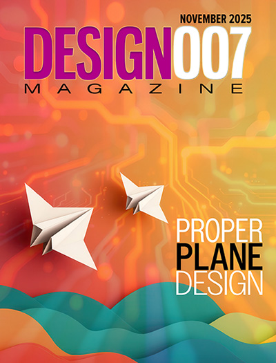
Designing Proper Planes
Without planes, designers would have to create thousands of traces to accomplish the same objectives. Power planes provide low impedance and stable power, and ground planes stabilize reference voltage, improve thermal performance, and help preclude EMI issues.

Power Integrity
Current power demands are increasing, especially with AI, 5G, and EV chips. This month, our experts share “watt’s up” with power integrity, from planning and layout through measurement and manufacturing.

Signal Integrity
If you don’t have signal integrity problems now, you will eventually. This month, our expert contributors share a variety of SI techniques that can help designers avoid ground bounce, crosstalk, parasitic issues, and much more.
- Articles
- Columns
- Links
- Media kit
||| MENU - design007 Magazine
The Gerber Guide, Chapter 2
October 5, 2015 | Karel Tavernier, UcamcoEstimated reading time: 2 minutes
It is clearly possible to fabricate PCBs from the fabrication data sets currently being used; it's being done innumerable times every day all over the globe. But is it being done in an efficient, reliable, automated and standardized manner? At this moment in time, the honest answer is no, because there is plenty of room for improvement in the way in which PCB fabrication data is currently transferred from design to fabrication.
This is not about the Gerber format, which is used for more than 90% of the world's PCB production. There are very rarely problems with Gerber files themselves; they allow images to be transferred without a hitch. In fact the Gerber format is part of the solution, given that it is the most reliable option in this field. The problems actually lie in which images are transferred, how the format is used and, more often, in how it is not used.
In this monthly series, I will explain in detail how to use the newly revised Gerber data format to communicate with your fabrication partners clearly and simply, using an unequivocal yet versatile language that enables you and them to get the very best out of your design data. Each month we’ll look at a different aspect of the design to fabrication data transfer process.
This column has been excerpted from the Guide to PCB Fabrication Data: Design to Fabrication Data Transfer.
Chapter 2: Alignment (Registration)
Never mirror or flip layers! All layers must be viewed from the top of the PCB, which means that the text must be readable on the top layer and mirrored on the bottom layer. Alas, sometimes, in a mistaken attempt to be helpful, designers flip layers because they must anyway be mirrored on the photoplotter. This could be helpful in a world where the designer's files are used directly in fabrication, but these data layers are actually input for the CAM system. This needs the correct 2.5D PC structure, so designers need to follow the standard protocol for providing digital data. The fabricator's CAM system will do the rest: it will optimise and panelise the PCB and on output of the final, panelised data, it will mirror, rotate, shift and scale as required by production. Any designer that mirrors layers can only hope that the CAM engineer notices this and ‘unmirrors’ them.
To read this entire article, which appeared in the September 2015 issue of The PCB Design Magazine, click here.
Testimonial
"The I-Connect007 team is outstanding—kind, responsive, and a true marketing partner. Their design team created fresh, eye-catching ads, and their editorial support polished our content to let our brand shine. Thank you all! "
Sweeney Ng - CEE PCBSuggested Items
NASH Industries Unveils its First Series of 'Make in India' Motherboards Powered by Intel's Raptor Lake Platform
11/25/2025 | PRNewswireNASH Industries recently announced the successful launch of its first series of 'Make in India' motherboards, designed and developed using the Intel B760 chipset for Intel's Raptor Lake (RPL) processor family.
Fairbanks Morse Defense to Acquire Truflo Marine from IMI
11/25/2025 | BUSINESS WIREFairbanks Morse Defense (FMD), a portfolio company of Arcline Investment Management, has entered into an agreement with IMI plc, to acquire its Birmingham, UK-based Truflo Marine business.
Target Condition: May I Take Your Order, Please?
11/26/2025 | Kelly Dack -- Column: Target ConditionAnyone who has ordered a car knows you don’t just stroll onto the lot, casually mention you want “a red one,” and drive away happy. There’s a process: You sit down with the dealer, pick your make and model, choose your options—engine size, interior trim, transmission type, sunroof—and agree on a price. Then the paperwork starts flying.
What Emerging Circularity Policies Mean for the Electronics Industry
11/20/2025 | I-Connect007 Editorial TeamAs Europe accelerates toward a circular economy, electronics manufacturers face a wave of new sustainability requirements that will redefine product design, materials management, and end-of-life strategies. During a Nov. 11 webinar co-hosted by the Global Electronics Association and the Anthesis Group, industry leaders outlined the regulatory landscape shaping the next decade, including the Eco-design for Sustainable Products Regulation (ESPR), the Right to Repair (R2R) Directive, and the Extended Producer Responsibility (EPR) regulatory framework.
TTCI Receives 2025 Global Technology Award for Redefining Design for Testability in High-Reliability Electronics
11/20/2025 | TTCIThe Test Connection Inc. (TTCI), a trusted provider of electronic test and manufacturing solutions, has been awarded the 2025 Global Technology Award in the Test Services category for its groundbreaking work in Design for Testability (DFT).


