


 The Marketing Minute: Marketing With Layers
 The Right Approach: Electro-Tek—A Williams Family Legacy, Part 1
 It’s Only Common Sense: If You’re Not Differentiated, You’re Dead


Practical Application of Lean Six Sigma to Drive Cycle Time Reduction, Part 1
October 22, 2015 | Kathy Nargi-Toth, NCAB Group USA Inc.Estimated reading time: 2 minutes
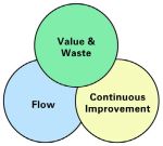
One of the most systematic and successful approaches to the challenge of cycle time reduction can be found in the principles and tools of lean six-sigma methodology. The success of this strategy requires commitment. It is not a quick fix, nor will it be effective if it is only used as an occasional housecleaning activity. To be successful requires a long-term commitment of time and resources and a tireless dedication to improvement. As a result you should expect and welcome change as your company focuses from inward (my product) to outward (my customer), with a goal of total customer satisfaction. It's a win-win solution.
Some might argue that Walter Shewhart was the inspiration for the concept of six sigma. It was Shewhart who in the 1920s identified common and special cause process change and introduced the control chart. The credit however for the term "six sigma" is given to Bill Smith and co-founder Dr. Mikel Harry of Motorola. In the mid-1980s, Motorola CEO Bob Galvin supported a quality initiative based on six sigma methodologies that changed the way Motorola did business, which improved quality, increased customer satisfaction and ultimately saved hundreds of millions of dollars in the process.
Motorola's six sigma concept began with four basic principles: measure, analyze, improve, control (MAIC). The D (define) of DMAIC was added later by GE. Today, six sigma includes lean principles as well as methods that introduce six sigma earlier into the design phase of the process, which enables faster time-to-market with products that better meet the customers’ specific requirements. By using six sigma principles and lean techniques together, PCB manufacturers can reduce both process variation and cycle time together effectively.
Getting Started
The PCB manufacturing process is by nature a batch process, following a predetermined sequence that is developed to meet the products’ specific design requirements. In PCB manufacturing not all products go through the exact same process, which complicates the task of cycle time reduction. As an example, a standard multilayer board will probably not be laser-drilled or plasma-etched unless it has some very unique characteristics. And HDI products may cycle through lamination, drilling, laser drilling, plating and etching two or more times before moving on to solder mask application. Cycle time reduction efforts for these two products will require individual evaluation.
Editor's Note: This article originally appeared in the October 2015 issue of SMT Magazine.
Share on:


Testimonial
"Advertising in PCB007 Magazine has been a great way to showcase our bare board testers to the right audience. The I-Connect007 team makes the process smooth and professional. We’re proud to be featured in such a trusted publication."
Klaus Koziol - atgSuggested Items
Indium Experts to Deliver Technical Presentations at SMTA International
10/14/2025 | Indium CorporationAs one of the leading materials providers to the power electronics assembly industry, Indium Corporation experts will share their technical insight on a wide range of innovative solder solutions at SMTA International (SMTAI), to be held October 19-23 in Rosemont, Illinois.
Knocking Down the Bone Pile: Revamp Your Components with BGA Reballing
10/14/2025 | Nash Bell -- Column: Knocking Down the Bone PileBall grid array (BGA) components evolved from pin grid array (PGA) devices, carrying over many of the same electrical benefits while introducing a more compact and efficient interconnect format. Instead of discrete leads, BGAs rely on solder balls on the underside of the package to connect to the PCB. In some advanced designs, solder balls are on both the PCB and the BGA package. In stacked configurations, such as package-on-package (PoP), these solder balls also interconnect multiple packages, enabling higher functionality in a smaller footprint.
Indium to Showcase High-Reliability Solder and Flux-Cored Wire Solutions at SMTA International
10/09/2025 | Indium CorporationAs one of the leading materials providers in the electronics industry, Indium Corporation® will feature its innovative, high-reliability solder and flux-cored wire products at SMTA International (SMTAI), to be held October 19-23 in Rosemont, Illinois.
‘Create your Connections’ – Rehm at productronica 2025 in Munich
10/08/2025 | Rehm Thermal SystemsThe electronics industry is undergoing dynamic transformation: smart production lines, sustainability, artificial intelligence, and sensor technologies dominate current discussions.
Amplifying Innovation: New Podcast Series Spotlights Electronics Industry Leaders
10/08/2025 | I-Connect007In the debut episode, “Building Reliability: KOKI’s Approach to Solder Joint Challenges,” host Marcy LaRont speaks with Shantanu Joshi, Head of Customer Solutions and Operational Excellence at KOKI Solder America. They explore how advanced materials, such as crack-free fluxes and zero-flux-residue solder pastes, are addressing issues like voiding, heat dissipation, and solder joint reliability in demanding applications, where failure can result in costly repairs or even catastrophic loss.