


 Connect the Dots: Designing for the Future of Manufacturing Reality—Strip-Etch-Strip
 Fresh PCB Concepts: Cost Stability in a Period of Copper and Gold Volatility
 Beyond the Board: The Benefits of Early PCB Engagement in Aerospace and Defense Programs


Mentor Graphics Unveils PADS PCB Product Creation Platform
May 3, 2016 | PRNewswireEstimated reading time: 4 minutes
Mentor Graphics Corporation today announced a comprehensive product-creation platform based on PADS PCB software that enables individual engineers and small teams to solve the engineering challenges involved in creating today's electronic products. With increasing systems design complexity and the need for printed circuit board (PCB), mechanical and systems engineers to access easy-to-deploy tools, the PADS platform has been extended to enable engineers to develop PCB-based systems from concept through manufacturing hand-off.
The product creation process is much more than schematic capture and board layout. Engineers must address many other issues for a successful product design, including component selection, signal and power integrity, electronic cooling, form and fit, and design for manufacturability. With this release, the PADS platform extends its product-creation solution by adding PADS HyperLynx® DC Drop and PADS FloTHERM® XT tools for high productivity at unprecedented price-performance.
"The complexity of systems design keeps climbing, as design teams continue to aim for higher levels of capability and performance in their products. Systems design for products of all types entails a host of electrical, mechanical, thermal and manufacturing complexities with which design teams must contend," said Laurie Balch, chief analyst, Gary Smith EDA. "It is essential for EDA vendors to help design engineers successfully tackle these issues through their design tools, as Mentor is demonstrating with its latest investment in its PADS platform portfolio."
"With increasing complexity in electronics systems, engineers need to develop with the whole product in mind," said Barry Olney, owner of In-Circuit Design. "Having access to a design tool that encompasses PCB design, coupled with comprehensive simulation and analysis, really gives design engineers the confidence that their products will be delivered on schedule and at the highest performance and reliability. At the end of the day, the PADS platform delivers a real competitive advantage."
DC Drop for Power Integrity Analysis
By adding world-class HyperLynx DC Drop analysis to the PADS platform, engineers can create electronic products ranging from low-power wearable devices to products that require high-power processors. The increasing number of power rails in modern devices can result in non-functional or hard-to-debug design if analysis isn't used early in the design process.
The PADS HyperLynx DC Drop product quickly identifies problem areas in the design which would be difficult to find in the lab on a prototype. The DC Drop tool quickly provides investigative solutions which the user can apply in an easy-to-use environment. Results can be validated in layout to ensure that appropriate guidelines were followed, thus reducing prototype spins. With the DC Drop product, engineers can:
- Optimize the power distribution network (PDN) for efficient, clean, multi-voltage power to ICs.
- Quickly analyze voltage drops caused by insufficient copper across power supply rails, thus eliminating time-consuming troubleshooting of prototypes.
- Identify layout areas that contain excessive current density so they can be eliminated early.
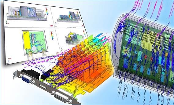
PADS FloTHERM XT Tool for Electronics Cooling
As electronics become smaller, faster, and more densely packaged, designers need to consider complete thermal effects to ensure product reliability. Physical testing is not always possible due to time and cost but, with the PADS product creation platform, a system's thermal profile requirements can be achieved quickly, easily, and affordably. The PADS FloTHERM XT product is an award-winning electronics cooling solution that can be used as early as placement to identify thermal effects of the entire system. Using the SmartParts™ feature, designers can build simple models in minutes, apply complex mechanical parts directly from MCAD, create custom CAD geometry with ease, and import detailed electronic assemblies from EDA tools.
Key benefits of PADS FloTHERM XT include:
- A CAD-centric solution for thermal simulation and electronic cooling.
- Consideration for all thermal aspects of the design, including package selection, PCB layout, board structure, and enclosure design.
- Direct interfaces with all major MCAD vendors and all vendor-neutral file formats.
- Automatic report generation via HTML, PDF, or Microsoft® Word.
"Mentor is unrivaled in delivering technology innovation that enables competitive advantage for our customers. With Xpedition for enterprises, to PADS for the mainstream market, our solutions portfolio continues to evolve allowing the market to tackle the most complex product creation challenges," stated A.J. Incorvaia, vice president and general manager of Mentor Graphics Board Systems Division. "Our new PADS release with thermal and voltage analysis capabilities provides an intuitive solution that helps individual electronic designers go from design concept through manufacturing."
Product Availability
The new PADS release with PADS HyperLynx DC Drop and PADS FloTHERM XT electronic cooling options will be available in July. The PADS HyperLynx DC Drop tool starts at $4995 (USD). The PADS FloTHERM XT tool starts at US$12,500.To learn more, consult a Mentor Graphics sales representative or call 1-800-547-3000. Additional product information can be found at www.pads.com.
About Mentor Graphics
Mentor Graphics Corporation is a world leader in electronic hardware and software design solutions, providing products, consulting services and award-winning support for the world's most successful electronic, semiconductor and systems companies. Established in 1981, the company reported revenues in the last fiscal year of approximately $1.18 billion. Corporate headquarters are located at 8005 S.W. Boeckman Road, Wilsonville, Oregon 97070-7777. Visit www.mentor.com.
Share on:


Testimonial
"Our marketing partnership with I-Connect007 is already delivering. Just a day after our press release went live, we received a direct inquiry about our updated products!"
Rachael Temple - AlltematedSuggested Items
Connect the Dots: Designing for the Future of Manufacturing Reality—Strip-Etch-Strip
02/19/2026 | Matt Stevenson -- Column: Connect the DotsThe demand for ultra-high density interconnect (UHDI) PCBs is growing as electronic devices become increasingly advanced. That means we will be creating more designs that need to align with the reality of manufacturing UHDI boards. My last column on this subject focused on plating, and we are ready to discuss the strip-etch-strip (SES) process. With UHDI boards, footprints are smaller and tolerances are tighter. Your big design challenge associated with the SES process involves trace width and spacing control. The etching process can undercut traces and alter their final size.
Powering the Future: From Thick-Film to DBC—Understanding the Evolution of Ceramic Packaging
02/11/2026 | Brian Buyea -- Column: Powering the FutureCeramic packaging has quietly powered the electronics revolution for more than half a century. From the earliest thick-film hybrids to today’s direct bond copper (DBC) substrates and metallized aluminum nitride, every step forward in ceramic technology has pushed the limits of reliability, power density, and performance. It’s essential for every design engineer building the next generation of electronic systems to understand this evolution.
Fresh PCB Concepts: Cost Stability in a Period of Copper and Gold Volatility
02/12/2026 | Team NCAB -- Column: Fresh PCB ConceptsAnyone who works with PCBs in any capacity right now can feel that copper and laminate prices are not stagnant, gold price is increasing even faster, and the impact shows up quickly on PCB quotations. For many design teams, this feels like a force outside their control. Raw materials go up, and the board cost goes with it. I want to highlight that many of these swings are manageable.
Connect the Dots: The Future of Designing for Reality—Pattern Plating
02/05/2026 | Matt Stevenson -- Column: Connect the DotsLast month, I discussed the outer-layer imaging process and offered tips for designers to help ensure smooth manufacturing and high-quality output. The next step in the manufacturing process is copper pattern plating, where fabrication can be tricky, and design precision is even more important. The board is now ready to have the copper traces, through-holes, vias, pads, and other elements specified in the original CAD design plated to copper thickness requirements. I will identify some key design considerations for pattern plating, break down the process, and offer design tips for a successful outcome.
PCBAIR Upgrades Heavy-Copper PCBs to Solve AI Thermal Bottlenecks
01/20/2026 | PRNewswireAs computational demands for AI models surge, the hardware powering them faces a critical physical limitation: thermal management.