-

-
News
News Highlights
- Books
Featured Books
- design007 Magazine
Latest Issues
Current Issue
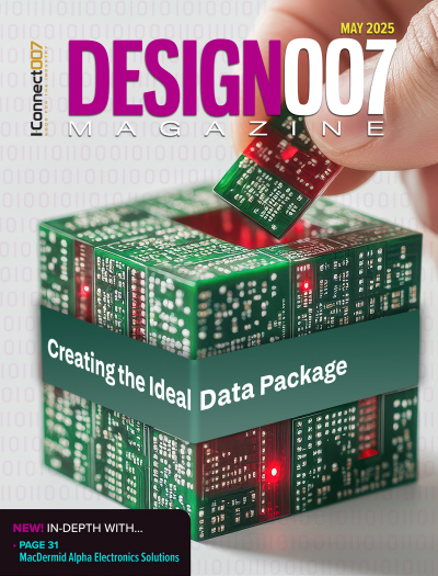
Creating the Ideal Data Package
Why is it so difficult to create the ideal data package? Many of these simple errors can be alleviated by paying attention to detail—and knowing what issues to look out for. So, this month, our experts weigh in on the best practices for creating the ideal design data package for your design.

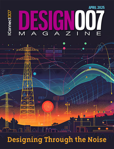
Designing Through the Noise
Our experts discuss the constantly evolving world of RF design, including the many tradeoffs, material considerations, and design tips and techniques that designers and design engineers need to know to succeed in this high-frequency realm.

Learning to Speak ‘Fab’
Our expert contributors clear up many of the miscommunication problems between PCB designers and their fab and assembly stakeholders. As you will see, a little extra planning early in the design cycle can go a long way toward maintaining open lines of communication with the fab and assembly folks.
- Articles
- Columns
Search Console
- Links
- Media kit
||| MENU - design007 Magazine
Beyond Design: The Case for Artificial Intelligence in EDA Tools
June 28, 2016 | Barry Olney, In-Circuit Design Pty LtdEstimated reading time: 2 minutes
I-Connect007 Editor Andy Shaughnessy reported that the keynote speaker at the IPC APEX EXPO Design Forum was Dean Parker, a former PCB designer at Shure who is now a CAD manager at Google X. Parker is involved in the development of autonomous vehicles and all sorts of other great ideas at Google X. According to Andy, Parker told the crowd, among other things, that EDA tool vendors need to trash all their old 1990s code and start over, this time with artificial intelligence.
There has been a lot of activity in the field of AI recently, with such developments as voice recognition, unmanned autonomous vehicles and data mining to list a few. But how could AI possibly influence the PCB design process? This month, I will take a look at the endless possibilities.
So much time is wasted on reproducing the same thing over and over again on each layout. Current EDA tools, with all their bells and whistles, are still very limited in automation processes and mostly rely on the skills and foresight of the engineer and PCB designer to drive the software through all the hoops. Instead, EDA tools need to predict what the designer is trying to do, then look at previous designs to suggest alternatives and auto-complete the design where possible. AI is a system that perceives its environment and takes actions to maximize its chances of success.
Automating many of the tedious steps in setting up the initial database would be a good start. A standard form factor could be used to establish the initial layout environment ensuring that designs are compatible across multiple generations of technology. Although some PCB layout tools allow the designer to load a standard set of predefined startup configuration files, there is still too much manual intervention required. The PCB database could predict the fundamental design rules and via stack requirements sourced from previous experience.
Predictive text, which we all use every day on our cell phones, could provide self-evident naming conventions for supplier part numbers and database fields, greatly speeding up the design definition. Busses and interfaces could be analyzed and categorized with naming conventions interpreted from the chip pin name assignments, eliminating much of the monotonous schematic capture process. IC power pins could have powers supplies assigned based on datasheet requirements. And a starter set of decoupling capacitors, added to each power pin, could kick off the PDN analysis based on previous capacitor availability and parameter selections.
A selection of predefined library components could be offered, based on an initial bill of materials, and pre-placed on the schematic predicting the designer’s requirements. IBIS models could be automatically assigned to each chip, based on the part number and all the interconnecting transmission lines identified. The IBIS model’s source and load impedances could be extracted to assign the required impedance and terminations to each individual transmission line.
Also from this, the board stackup could be created based on previous designs, with similar technology, selecting dielectric materials, from a well maintained library, sourced from the preferred fabricator availability, dielectric loss and bandwidth requirements. Data and address busses together with clock/strobe different pairs, defined at the schematic entry level, could be assigned to certain layers in order to minimize crosstalk, electromagnetic emissions and return path loops. Power plane shapes could be automatically defined based on component placement and on the pins that need to be connected, allowing for DC drop and maximum current supply.
To read this entire article, which appeared in the May 2016 issue of The PCB Design Magazine, click here.
Suggested Items
Polar Brings New Book 'The PCB Designers Guide to... More Secrets of High Speed PCBs' to EIPC Edinburgh
05/27/2025 | Polar InstrumentsPolar's latest book, The PCB Designer's Guide to... More Secrets of High Speed PCBs, will see its European Launch at the EIPC conference in Edinburgh, June 3-4, 2025. More Secrets unveils more of the knowledge that is often missed from theoretical text books to help both new and experienced designers realize the PCBs they “thought” they had designed.
FastlinkPCB Accelerates Global Expansion, Builds Efficient PCB Industry Chain
05/26/2025 | FastlinkPCBFastlinkPCB, a PCB manufacturing and assembly solutions provider, announced that it has completed the layout of subsidiaries in the US, Germany, Switzerland, and Malaysia over the past year, forming a localized service network covering North America, Europe, and Southeast Asia.
Defining the Ideal PCB Design Data Output
05/27/2025 | Stephen V. Chavez, Siemens EDAAt the heart of delivering successful, manufacturable printed circuit boards lies a vital question: What should your design data output package include to best support manufacturing? The answer: It depends. There are many factors to consider regarding the specific category you’re designing for—such as mil/aero, space, medical, and commercial. Other factors that need to be considered are requirements and engineering intent.
Indium to Feature Materials Solutions for Semiconductor Packaging and Assembly at ECTC
05/22/2025 | Indium CorporationIndium Corporation®, an industry leader in innovative materials solutions for semiconductor packaging and assembly, will feature its lineup of high-reliability products at the Electronics Component and Technology Conference (ECTC), taking place May 27-30 in Dallas, Texas.
HBM4 Raises the Bar on Manufacturing Complexity, Premium Expected to Exceed 30%
05/22/2025 | TrendForceTrendForce's latest findings reveal that demand for AI servers continues to accelerate the development of HBM technologies, with the three major suppliers actively advancing their HBM4 product roadmaps.


