


 Global Sourcing Spotlight: Building a Supply Chain That Bends, Not Breaks
 Smart Automation: The Journey of a Component Through an SMT Factory
 Powering the Future: Why Thermal Management Defines the Future of Electronics


The Root Causes & Solutions for Warped PC Boards
September 27, 2017 | Duane Benson, Screaming CircuitsEstimated reading time: 2 minutes

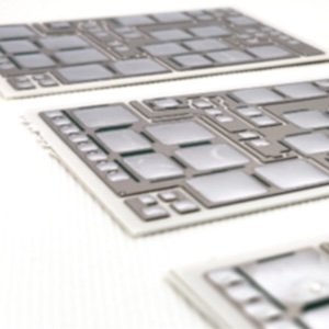
So, you just got a nice big PCB back from the fab shop. You set one on your desk to admire, only to discover that it's warped. What do you do?
There are two primary types of causes of board warping: process related at the fab or assembly shop, and layout related issues.
If it's warped before assembly, it's between fab and layout. If it's flat before assembly and warped after, it's most likely between layout and assembly. That said, sometimes a fab problem won't show up until a pass through the reflow oven at your assembly partner.
Determining the root cause is generally a bit of an iterative process. It's tempting to start right off with your fab or assembly partner, but you need some information before giving them a call. You'll need such things as the amount of warpage per inch, board size and thickness. With that, you need to take a good look at your design and consider copper pours, component size and component placement.
With that information in hand, you can make your phone call. If the board is warped before assembly, call your fab shop. If it's flat pre-assembly and warped post assembly, call your assembly house.
The shop you call will want to talk over your design to help you pinpoint the cause. If you can rule out a design issue, then you need to talk with your partner to determine whether it's a fab or assembly issue, and the next steps to take care of you.
Here are a few design issues that could contribute to warping:
- Uneven copper pour: Copper and FR-4 are a good match relative to thermal expansion, but they aren't exact. A large pour on one side or corner of your board can lead to warping due to dissimilar expansion characteristics. This could cause warpage either at the fab shop or the assembly house.
- Thermal mass: Components with large thermal mass grouped together on the board. This would be more likely to cause problems during assembly than during fab. The thermal mass will act as a heat sink for that area on the board, which can lead to uneven expansion and uneven soldering.
- Thin boards: A board that's too thin for the size or number of components could lead to warping at any stage.
- Irregular shapes: Odd shapes or large cutouts could also lead to warping at any point.
There may be other, more obscure causes, but those are the main design related causes. If it's none of those, talk with your partner. Occasionally, design requirements lead to a board that is essentially non-manufacturable. Hopefully, you never have this situation, but if you do, make sure that thickness, component location, pours, or cut outs really need to be the way they are.
If you absolutely, positively can't change anything, go back and try again. Then you can to look for heroic means to get the board fabricated and built. Slight warpage might go away when the board is mounted. Just be careful. Some components may not stay securely soldered when you flatten it.
The board may need a special fixture during assembly to prevent warping. This will likely cost extra, but if you can't change your design, and still need it built, it may be your best option.
Finally, if nothing works, you may need to look harder at the design, or look for a new fab or assembly house. We all like to think we can do just about anything, but every shop has its limits, and on rare occasion, those limits can be difficult to spot.
Share on:


Testimonial
"We’re proud to call I-Connect007 a trusted partner. Their innovative approach and industry insight made our podcast collaboration a success by connecting us with the right audience and delivering real results."
Julia McCaffrey - NCAB GroupSuggested Items
Driving Innovation: Selecting the Right Laser Source
04/28/2026 | Simon Khesin -- Column: Driving InnovationWhen I first joined Schmoll Maschinen, I brought experience from almost every PCB process, except for laser. As I immersed myself in laser processing, I realized why it can seem so daunting to a newcomer. The complexity arises from three intersecting factors: A vast variety of laser sources: CO2, UV-nano, green-pico, UV-pico, IR-pico, and others; a diverse range of applications: Drilling, cutting, ablation, and more; and an extensive list of materials: These have vastly different absorption rates. Choosing the right machine or laser source is rarely trivial. Even for experienced engineers, answering "Which source is best?" requires examining the business's specific goals.
Institute of Circuit Technology Spring Seminar 2026: A Bright Future in Europe
04/23/2026 | Pete Starkey, I-Connect007Through the leafy lanes and spring flowers of Warwickshire and back to Meridan, the traditional centre of England, and now officially part of the Metropolitan Borough of Solihull in the county of the West Midlands, I attended the Annual General Meeting and Spring Seminar of the Institute of Circuit Technology (ICT) on April 14. Out of the AGM came notable changes in leadership at the top of the Institute: the retirement of Mat Beadel as chair and Emma Hudson as technical director. Effective May 1, Steve Driver is the new chair, and Alun Morgan is the new technical director.
ACCM Unveils Negative and Near-zero CTE Materials for Large-Format AI Chips
04/21/2026 | Advanced Chip and Circuit MaterialsAdvanced Chip and Circuit Materials, Inc. (ACCM) has launched two new materials: Celeritas HM50, with a negative coefficient of thermal expansion (CTE) of -8 ppm/°C to offset the positive CTE and expansion of copper with temperature on circuit boards, and Celeritas HM001, with near-zero CTE and the low-loss performance needed for high-speed signal layers to 224 Gb/s and faster in artificial intelligence (AI) circuits.
Fresh PCB Concepts: Designing PCBs for Harsh Environments—Reliability Is Engineered Upstream
04/23/2026 | Team NCAB -- Column: Fresh PCB ConceptsWhen engineers hear the phrase “harsh environment,” they usually think of the extreme temperature swings, vibration and shock, pressure changes, or radiation in aerospace. However, aerospace is not the only harsh environment where electronic assemblies must survive. Automotive power electronics, downhole oil and gas tools, marine controls, rail systems, defense platforms, and industrial automation equipment all expose PCBs to environments that are equally unforgiving. The stress mechanisms may differ, but the physics does not.
Advanced Packaging for AI: Reliability Starts at the Cu/Cu/Cu Microvia Junction
04/20/2026 | Kuldip Johal, MKS' AtotechThe rapid growth of AI computing, from training clusters to inference at scale, is reshaping demand across the entire electronics supply chain. Advances in technology requirements, such as higher bandwidth, lower latency, and greater compute density, are driving the development of advanced packaging technologies and transforming the PCB industry across design, manufacturing, testing, and even architecture.