


 Learning with Leo: Drones—Meeting Demand Without Compromise
 Nolan’s Notes: Our Spotlight on North America
 Global Sourcing Spotlight: Building a Supply Chain That Bends, Not Breaks


Process, Design and Material Factors for Voiding Control for Thermally Demanding Applications
November 6, 2018 | Ranjit Pandher, et al., Alpha Assembly SolutionsEstimated reading time: 4 minutes
Solder voiding is a common phenomenon across all semiconductor packaging and electronic board assemblies. Voids are a troublesome defect in assemblies created using surface mount technology. Voids can interfere with electric signals, can be insulators when heat dissipation is required, and they can also be the source of crack propagation and early failure of an assembly when occurring near the pad surface. The acceptable levels for voiding vary upon on the end-application and environment it's used in. In the case of thermally demanding harsh environment applications such as automotive and outdoor LED lighting, void control is required in order to optimize the performance and extend the lifetime of these components. The lower the voiding on these thermal and electrical pads, the better the connection to the PCB and subsequent layers.
There are many factors that influence void frequency and size. This study focuses on several process, design and materials selection considerations which control or potentially reduce voiding to meet industry and end-market acceptance criteria. More specifically, package design, reflow profiles, and solder paste chemistry are discussed in the form of application studies. Commercial mid-power PLCC and high-power ceramic LED packages on aluminum metal core PCBs additionally BGA, D-Pak, and MLF on FR4 PBCs were used for these case studies.
Figure 1: Void entrapment within the solder layer.
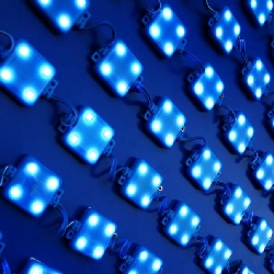
The global acceptance of LED-based light sources has propelled the energy efficient technology to enter numerous markets and end applications including high power lighting segments. Examples include exterior automotive headlamps, roadway/street lighting, industrial high bay lights, architectural and entertainment lighting. As a result, customer expectations of maintaining efficiency, government regulations, safety, and reducing overall systems/replacement costs are important to satisfy the adoption rates.
For these high reliability and lifetime requirements, it is critical to have excellent assembly interconnect reliability to address the above needs.
The role of interconnects in LED Level 1 (chip/die attach) and Level 2 (package on board attach) is fundamentally to:
- Convey power and information efficiently and reliably over the rated life
- Thermal management—get the heat out faster and reliably over the rated life.
- Enable more light output, consistently, for longer time for the same package and system footprint.
- Capable of being processed under robust processing conditions i.e. multiple reflow assembly.
Figure 2: High-power LED heat path.
Voids, which are pockets of trapped gasses from solder flux, can cause issues for electric signals, can act as thermal resistors when heat dissipation is required, and they can also be the source of crack propagation and early failure of an assembly. Figure 1 depicts large area voids in the bulk solder layer. The phenomenon of void occurrence is a complex system; there are many factors that drive various levels of voiding. Examples include: chemistry, reflow profile, volume of material, solderable pad finish and design of the component pads (thermal and electrical).
For level 1 LED chip attach assemblies the use of traditional solders can be seen as an advantage from both ease of processing and cost. However, the importance for thermal management is critical for high and ultra-high-power LEDs. The junction temperature in the LED increases with increasing drive current. Since more than 50% of electrical input power is dissipated as heat due to efficiency droop at high drive currents in LEDs, this rise in the junction temperature reduces the light output by increasing the probability of non-radiative recombination causing drop in efficiency and rated lifetime. Therefore, the dissipated heat needs to be removed from the junction in order to maintain the light conversion efficiency and light output from the high-power LED package. The various components in the heat flow path in a high-power LED package are shown in Figure 2.
Table 1: Test vehicle details.
Additionally, for Level 1, the requirements for processing LED packages with solder-based die attach on boards as a Level 2 assembly requires multiple soldering reflow capability. With multiple reflows of the same solder bulk layer, this may increase the levels of voids impacting the overall reliability of the stack at the Level 1 layer.
For Level 2 package on-board assemblies LEDs are becoming more integrated with various traditional IC components such as BGAs, D-Paks and MLFs being directly mounted on the same board. This is driven by the need for lighting systems to go beyond general illumination providing more complex features such as control, sensing and modulation. Large area voids can create issues in the electrical signal or generate cracks due to thermal cycling/fatigue thus need for a more robust, low voiding interconnects are required at the Level 2 layer.
Table 2: LED pad dimensions (mm).
Experimental Procedure – Design Case
Table 3: Print conditions.
There are a variety of LED designs used in the industry ranging from design structure/size and package materials i.e. ceramic and plastic. The goal of this experiment is to observe the effect of voiding based on three varying structures with the key difference being the pad geometries. For example, a 2-pad design where the anode and cathode are symmetrical, a 3-pad high aspect ratio design where the central thermal pad is slightly larger in terms of total area and lastly, a 3-pad design where the central thermal pad is significantly larger in terms of total area when compare to the anode and cathode. Table 2 shows the total area and construction of the LED pads.
ASSEMBLY MATERIALS & COMPONENTS
Substrate
The substrate used in this study is a custom designed aluminum core PCB. The particular details for this board are shown in Table 1.
LED Components
For this study, three commercially available high-power LEDs were selected with varying pad geometries. The parameters for anode, cathode, and thermal pad dimensions for the LEDs are listed in Table 2. All dimensions are in millimeters. The LEDs were chosen to emulate common packages selected in high and ultra-high-power assemblies.
Solder Pastes
A commercially available no-clean solder paste was used for this study known using a type 4 particle size SAC-based alloy (38–20 Particle size in µm (80% min. between)).
PROCESS AND TEST METHOD
Equipment Processing Details
Solder paste printing was done using DEK Horizon 03iX printer with a 4 mil thick laser cut stainless steel stencil with a 1 to 1 ratio of aperture size to pad size. Stencil printing parameters used for all solder pastes are shown in Table 3.
Reflow Soldering
The soak reflow profile was used in this study shown in Figure 2 the temperatures are displayed in Table 4.
Table 4: Reflow profile used in study.
Test Method
To measure and quantify the voiding performance of the varying pastes and LED pad layouts, the assembled and reflowed boards were loaded into an X-ray analysis unit and programmed to quantify the area of each void as a percent of the total pad area and the number of voids under the package.
To read the full article, which appeared in the October 2018 issue of SMT007 Magazine, click here.
Visit I-007eBooks to download your copy of Alpha's micro eBook today:
The Printed Circuit Assembler’s Guide to… Low-Temperature Soldering
Share on:


Testimonial
"Advertising in PCB007 Magazine has been a great way to showcase our bare board testers to the right audience. The I-Connect007 team makes the process smooth and professional. We’re proud to be featured in such a trusted publication."
Klaus Koziol - atgSuggested Items
BGA Technology Expands Inspection Capabilities with Creative Electron TruView X-ray System
05/08/2026 | BGA TechnologyBGA Technology, a leading provider of advanced electronics testing and inspection services, has enhanced its inspection capabilities with the addition of a Creative Electron TruView™ Simplex X-ray system at its Holbrook, New York facility.
AQUANOX A4727 and A4625 Lead KYZEN Offerings at SMTA Oregon Expo and Tech Forum
05/06/2026 | KYZENKYZEN, the global leader in innovative environmentally responsible cleaning chemistries, will exhibit at the SMTA Oregon Expo and Tech Forum scheduled to take place Thursday, May 19 at the Wingspan Event and Conference Center in Hillsboro, Oregon.
Connect the Dots: Designing for the Future of Manufacturing Reality—Surface Finish
05/07/2026 | Matt Stevenson -- Column: Connect the DotsWhen designing the complex boards that many electronic devices require to operate, designers should consider manufacturability at every step. This is my last article focused on designing for the always-evolving manufacturing reality. Choosing the right surface finish has always been important. If you are creating intricate designs with a wide variety of components, like for an ultra-high density interconnect (UHDI) board, surface finish is a critical last step.
Indium to Showcase High-Performance AI Application Solutions at SEMICON SEA 2026
05/01/2026 | Indium CorporationAs a leading provider of advanced materials solutions for today’s demanding AI applications, Indium Corporation® will feature its high-reliability product portfolio at SEMICON SEA 2026, May 5-7, in Kuala Lumpur, Malaysia.
ACCM Unveils Negative and Near-zero CTE Materials for Large-Format AI Chips
04/21/2026 | Advanced Chip and Circuit MaterialsAdvanced Chip and Circuit Materials, Inc. (ACCM) has launched two new materials: Celeritas HM50, with a negative coefficient of thermal expansion (CTE) of -8 ppm/°C to offset the positive CTE and expansion of copper with temperature on circuit boards, and Celeritas HM001, with near-zero CTE and the low-loss performance needed for high-speed signal layers to 224 Gb/s and faster in artificial intelligence (AI) circuits.