


 Designer’s Notebook: What Designers Need to Know About Manufacturing, Part 2
 The Pulse: Drilling Down on Documentation
 Connect the Dots: Designing for Reality: Prioritizing Manufacturability
Ansys, Electro Magnetic Applications Launch EMA3D Charge
October 21, 2021 | ANSYSEstimated reading time: 2 minutes
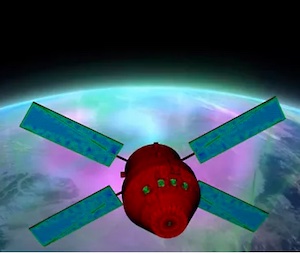
Together with Electro Magnetic Applications, Ansys added EMA3D Charge to its industry-leading simulation solution portfolio, addressing critical design and safety needs for applications ranging from space exploration to everyday commutes. The new solution enhances predictive accuracy for engineers analyzing charging and discharging events that can lead to catastrophic product failures early in the design cycle, driving faster time-to-market and bottom-line savings.
Aerospace, electronics and automotive industries must meet rigorous electrical performance requirements to mitigate safety risks related to charging and discharging events. Engineers need to be confident a spacecraft will survive exposure to space plasma. High-voltage systems must operate safely without risk of fire. Autonomous vehicles must maintain safety critical functions when faced with an unexpected electrical event. Without fully understanding and addressing these risks, companies may face costly late-phase redesigns, often totaling millions of dollars.
High-fidelity predictions from EMA3D Charge provide engineers with a deeper understanding of electrical charging and discharging phenomena. These insights can have a significant impact on product design, helping engineers determine how electrical components may be harmed — and to what extent — by charging and discharging events. Mitigating risks early in the design phase reduces the chances of late-stage redesigns and costly product failures.
“EMA3D Charge has an impressive array of capabilities,” said EMC engineers at NASA Johnson Space Center. “For example, its ability to easily manipulate and mesh mechanical computer-aided design (CAD) models greatly simplifies the process of going from a structural model of the spacecraft to analytical results. We have also seen great value in its ability to perform charging analysis on spacecraft that are being charged by direct contact with lunar dusts whilst simultaneously being charged from exposure to space plasmas on or near the lunar surface.”
While the technology within EMA3D Charge has been applied in the electronics and aerospace industry before, the solution is the first to be focused entirely on charging and discharging prediction. Leveraging Ansys SpaceClaim to create an intuitive user interface and workflow, EMA3D Charge combines CAD import, design and simplification, simulation setup and meshing, and result generalization and visualization into one solver technology.
“EMA3D Charge fills a need in a marketplace in which no other simulation product exists,” said Shane Emswiler, senior vice president of products at Ansys. “Engineers simulating charging and discharging events once had to navigate multiple codes and challenging workflows that fell short of a full solution. EMA3D Charge is a full solution—one that provides high-fidelity analysis and an end-to-end workflow designed for efficiency.”
Share on:


Suggested Items
Real Time with… IPC APEX EXPO 2024: My Role as a Technology Solutions Director
05/02/2024 | Real Time with...IPC APEX EXPOPeter Tranitz, senior director of technology solutions at IPC, shares insights into his role as the design initiative lead. He details his advocacy work, industry support, and the responsibilities of the design initiative committee. The conversation also covers the revamping of standards, the IPC Design Competition, and the implementation of design rules in software tools.
Real Time with… IPC APEX EXPO 2024: Ventec Discusses New Pro-bond Family of Advanced Products
05/01/2024 | Real Time with...IPC APEX EXPOChris Hanson, Ventec's Global Head of IMS Technology, outlines the launch of four pro-bond formulas that deliver an outstanding combination of low dissipation factor (Df) with a dielectric constant (Dk) range to maximize the design window for critical PCB parameters. As Chris points out, Pro-bond is designed for low-loss, high-speed applications, while thermal-bond dissipates heat from a component through the board to a heat sink.
IPC's Vision for Empowering PCB Design Engineers
04/30/2024 | Robert Erickson, IPCAs architects of innovation, printed circuit board designers are tasked with translating increasingly complex concepts into tangible designs that power our modern world. IPC provides the necessary community, standards framework, and education to prepare these pioneers as they explore the boundaries of what’s possible, equipping engineers with the knowledge, skills, and resources required to thrive in an increasingly dynamic field.
On the Line With… Talks With Cadence Expert on SI/PI for PCB Designers
05/02/2024 | I-Connect007In “PCB 3.0: A New Design Methodology—SI/PI for PCB Designers,” subject matter expert Brad Griffin, Cadence Design Systems, discusses how an intelligent system design methodology can move some signal and power integrity decision-making into the physical design space, offering real-time feedback.
iNEMI Packaging Tech Topic Series: Role of EDA in Advanced Semiconductor Packaging
04/26/2024 | iNEMIAdvanced semiconductor packaging with heterogenous integration has made on-package integration of multiple chips a crucial part of finding alternatives to transistor scaling. Historically, EDA tools for front-end and back-end design have evolved separately; however, design complexity and the increased number of die-to-die or die-to-substrate interconnections has led to the need for EDA tools that can support integration of overall design planning, implementation, and system analysis in a single cockpit.