


 Knocking Down the Bone Pile: Revamp Your Components with BGA Reballing
 Global Sourcing Spotlight: Balancing Speed and Flexibility Without Sacrificing Control
 SMT Perspectives & Prospects: Artificial Intelligence Part 6: Data Module 1


Alpha Takes the Greenfield Route
February 28, 2023 | Nolan Johnson, I-Connect007Estimated reading time: 2 minutes

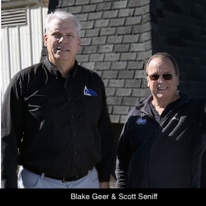
Alpha Circuit is a PCB fabricator located in Elmhurst, Illinois. Given that the launch of a new PCB fab is a rare occasion these days, we caught up with the senior team—Prashant Patel, president and CEO; Steve Smith, general manager; Steve Ryan, sales and direct support—guiding the buildout of Alpha Circuit’s brand new 44,000 square foot facility. They discuss what goes into equipment selection and line design, and the timing couldn’t have been better. At press time, the new facility was on schedule for test production by the end of January 2023.
Throughout the conversation, the Alpha team shared its methods for designing the facility, the parts of the fabrication process that are critical to get exactly right, and where the surprises were in the process.
Nolan Johnson: Gentlemen, welcome, and congratulations on your new facility. Let’s start with a little background about the company.
Steve Ryan: Alpha Circuit started in 1981, as a single- and double-sided board shop. Zenith was one of our big customers early on. We did a lot of punching and crunching back then and it is what really catapulted the revenue stream for us. When I joined the company in 2009, we were comfortably an eight to 12-layer multilayer and double-sided manufacturer. In 2013, we started doing flex and rigid-flex, increased our multilayers up to 28 layers, and started manufacturing copper-based pedestal-type design work.
Prashant Patel: When I acquired the company in 2020, my vision was to continue Alpha Circuit the way it was, while building a new facility to meet the higher technology demands. We purchased and renovated a 44,000 square foot facility, then ordered the equipment. It takes a long time to source equipment—you get the quotes, have it installed, and then get it running up to speed. That process has taken us over three years.
Steve Smith: I joined the company approximately two months ago. My background is HDI: stacked microvias, staggered microvias, along with high-speed digital materials, low-loss materials. I was hired to put the technology part of it together, getting the proper people and processes in place, so we can handle microelectronics down to 25-micron line and space and down to 3-mil pads.
Johnson: Great, thank you for that. Now, I want to talk today about your recent equipment purchases.
Smith: We have purchased a laser drill, and we have brand-new 200,000 RPM drill machines in place to do high aspect ratio holes. We also have a brand-new plating line with state-of-the-art chemistries to be able to do copper fill and through-hole plating in the same process along with being able to manufacture stacked vias starting with a 2-mil core substrate and stacking up to seven or eight lamination cycles.
To read this entire conversation, which appeared in the February 2023 issue of SMT007 Magazine, click here.
Share on:


Testimonial
"Your magazines are a great platform for people to exchange knowledge. Thank you for the work that you do."
Simon Khesin - Schmoll MaschinenSuggested Items
Episode 6 of Ultra HDI Podcast Series Explores Copper-filled Microvias in Advanced PCB Design and Fabrication
10/15/2025 | I-Connect007I-Connect007 has released Episode 6 of its acclaimed On the Line with... American Standard Circuits: Ultra High Density Interconnect (UHDI) podcast series. In this episode, “Copper Filling of Vias,” host Nolan Johnson once again welcomes John Johnson, Director of Quality and Advanced Technology at American Standard Circuits, for a deep dive into the pros and cons of copper plating microvias—from both the fabricator’s and designer’s perspectives.
Nolan’s Notes: Tariffs, Technologies, and Optimization
10/01/2025 | Nolan Johnson -- Column: Nolan's NotesLast month, SMT007 Magazine spotlighted India, and boy, did we pick a good time to do so. Tariff and trade news involving India was breaking like a storm surge. The U.S. tariffs shifted India from one of the most favorable trade agreements to the least favorable. Electronics continue to be exempt for the time being, but lest you think that we’re free and clear because we manufacture electronics, steel and aluminum are specifically called out at the 50% tariff levels.
MacDermid Alpha & Graphic PLC Lead UK’s First Horizontal Electroless Copper Installation
09/30/2025 | MacDermid Alpha & Graphic PLCMacDermid Alpha Electronics Solutions, a leading supplier of integrated materials and chemistries to the electronics industry, is proud to support Graphic PLC, a Somacis company, with the installation of the first horizontal electroless copper metallization process in the UK.
Electrodeposited Copper Foils Market to Grow by $11.7 Billion Over 2025-2032
09/18/2025 | Globe NewswireThe global electrodeposited copper foils market is poised for dynamic growth, driven by the rising adoption in advanced electronics and renewable energy storage solutions.
MacDermid Alpha Showcases Advanced Interconnect Solutions at PCIM Asia 2025
09/18/2025 | MacDermid Alpha Electronics SolutionsMacDermid Alpha Electronic Solutions, a global leader in materials for power electronics and semiconductor assembly, will showcase its latest interconnect innovations in electronic interconnect materials at PCIM Asia 2025, held from September 24 to 26 at the Shanghai New International Expo Centre, Booth N5-E30