


 Global Sourcing Spotlight: Golf, Friedman, and the Benefits of Global Sourcing
 Nolan’s Notes: Coming to Terms With AI
 The Knowledge Base: A CM’s Perspective on Box Build Practices
Koh Young Shares Revolutionary Advanced Package Inspection Solutions at the SMTA Wafer-Level Packaging Symposium
January 23, 2024 | Koh YoungEstimated reading time: 2 minutes
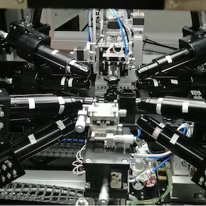
Koh Young Technology, the leader in True3D™ measurement-based inspection solutions, will be speaking at the SMTA Wafer-Level Packaging Symposium in Burlingame, California on our Multimodal Phase Shift Optics Approach to revolutionize high-speed 3D reconstruction of semiconductor and advanced packages. In the presentation will highlight how high-speed 3D reconstruction addresses the growing demand for electronic components, which necessitates fast and efficient processing. These advancements in measurement technology and AI integration have paved the way for enhanced packaging applications in the semiconductor industry.
During the event on Tuesday, 13 February 2024, Dr. Seung Hyun Lee, Ph.D. will present the paper “High-Speed Die and Component 3D Reconstruction Solution by Multimodal Phase Shift Optics Approach”. Therein he will explain how advancements in optical 3D measurement and the integration of Artificial Intelligence (AI) have paved the way for advanced packaging applications. Multi-modal measurement probes, equipped with enhanced depth of focus, can cover height differences in the latest package designs. Various surface conditions of components, chips, and surfaces are measured by combining an oblique optical system, which ensures stable high-speed measurement of objects with diffuse reflection, with a coaxial optical system, suitable for measuring objects with specular reflection. The integration of AI deep learning technology enables effective processing of various noises encountered during the measurements.
The SMTA WLPS will explore the massive changes in advanced package technology because electrical system architects are directly driving package performance requirements, something which has never happened before. Previously System Architects designed circuits around package limitations because pushing package technologies outside of their “comfort zones” often led to undesirable results. With the rise in transistor costs and the need to improve power efficiency, Silicon Architects have little choice but to push advanced package technologies well beyond their comfort zones.
The Wafer-Level Packaging Symposium will bring together the semiconductor industry’s most respected authorities to address all aspects of wafer-level, 3D device packaging, advanced manufacturing & test technologies. Addressing wafer-level packaging, 3D, and Advanced Manufacturing & Test technologies, the Wafer-Level Packaging Symposium will be at the forefront of packaging technology evolution. The conference will feature attendees from around the globe in the heart of Silicon Valley to immerse themselves in the latest technology and business trends. Register today at www.smta.org/mpage/wafer-register.
Other content from Koh Young:
- The Printed Circuit Assembler’s Guide to… SMT Inspection: Today, Tomorrow, and Beyond by Brent Fischthal. (Download the companion guide here.)
- I-007e Micro Webinar Series: “Smarter Manufacturing Enabled with Inspection Data” by Joel Scutchfield
You can view other titles in the I-007eBooks library here.
Share on:


Suggested Items
MKS’ Atotech to Participate in ECTC
05/10/2024 | MKS’ AtotechAt this year’s 74th IEEE Electronic Components and Technology Conference (ECTC), MKS’ Atotech will present and demonstrate its latest product and service innovations.
ZESTRON Academy Launches 2024 Advanced Packaging & Power Electronics Webinar Series
05/01/2024 | ZESTRONZESTRON, the leading global provider of high-precision cleaning products, services, and training solutions in the electronics manufacturing and semiconductor industries, proudly announces the launch of its highly anticipated webinar series on Advanced Packaging & Power Electronics, a webinar series on the latest innovations, cleaning, and corrosion challenges.
NextFlex Convenes the Hybrid Electronics Community at Binghamton University
05/01/2024 | NextFlexBinghamton University hosted the NextFlex hybrid electronics community on April 18 for a day of expert presentations, breakout sessions on technology and manufacturing topics, and networking.
Koh Young Extends Invitation to the 2024 IEEE Electronic Components and Technology Conference
04/30/2024 | Koh YoungKoh Young, the industry leader in True3D measurement-based inspection solutions, invites you to join us at the at the 2024 IEEE Electronic Components and Technology Conference from May 28-31, 2024, in Denver, Colorado at the Gaylord Rockies Resort & Convention Center.
iNEMI Packaging Tech Topic Series: Role of EDA in Advanced Semiconductor Packaging
04/26/2024 | iNEMIAdvanced semiconductor packaging with heterogenous integration has made on-package integration of multiple chips a crucial part of finding alternatives to transistor scaling. Historically, EDA tools for front-end and back-end design have evolved separately; however, design complexity and the increased number of die-to-die or die-to-substrate interconnections has led to the need for EDA tools that can support integration of overall design planning, implementation, and system analysis in a single cockpit.