


 One World, One Industry: Mastering Technology Prognostication
 Marcy's Musings: Charting the Future
 It’s Only Common Sense: Training Great Customer Service Reps
Researchers See "Spin Current" in Motion for the First Time
September 11, 2015 | SLAC National Accelerator LaboratoryEstimated reading time: 3 minutes
Researchers at the Department of Energy’s SLAC National Accelerator Laboratory have for the first time seen a spin current – an inherent magnetic property common to all electrons – as it travels across materials. The result, which revealed a surprising loss of current along the way, is an important step toward realizing a next-generation breed of electronics known as “spintronics.”.
Modern computing relies on the precise control of electric charges that zip around from component to component in labyrinth-like channels in semiconductors. Spintronics could change that by tapping electrons’ spin, which can be thought of as having an “up” or “down” orientation, rather than their charge.
Finding a way to directly control this up or down property, which is analogous to the magnetically stored zeros or ones in computer hard drive data, would rule out the need to flow electric charge in computer chips. Devices like laptops and smartphones would use less battery power and wouldn’t get so hot during use, and could also access data more quickly.
But the movement of this magnetic spin current had only been measured indirectly until a SLAC-led team found a way to directly observe it using X-rays. Their work, featured on the cover of the Aug. 28 edition of Physical Review Letters, could prove useful in guiding the selection of materials to improve spintronics performance.
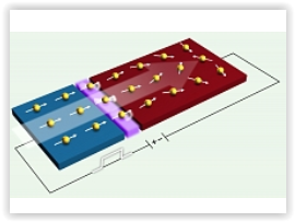
Image - The Aug. 28, 2015, edition of Physical Review Letters features an illustration from a Stanford Synchrotron Radiation Lightsource scientific result.“It’s really a magnetic needle in a haystack,” said Hendrik Ohldag, a staff scientist at SLAC’s Stanford Synchrotron Radiation Lightsource (SSRL) who participated in the research. SSRL is a DOE Office of Science User Facility. The research team, which included researchers from industry, created a spintronics test device that flowed the spin current from a cobalt-based magnetic material across copper, a nonmagnetic material.
“What we really didn’t know was how this magnetization flowed from one material to another,” Ohldag said, “and that is what we saw for the first time.”
Simply seeing this spin-related current in the copper material was an important achievement, Ohldag said, but researchers also found that the current loses more than half of its magnetic spin strength as it travels from the magnetic material to the nonmagnetic material.
“We see that most of the magnetization gets lost here at the interface between the two materials,” added Roopali Kukreja, lead author of the paper and a graduate student at Stanford University at the time the experiments were performed. “This was an ‘Oh, wow!’ moment because nobody had suspected this. The copper atoms at the interface are almost magnetic, and that is where you really lose the spin property of this current. The role of this interface was not clear before.”
To make spintronics devices more effective for commercial applications, Ohldag said researchers will need to limit this loss of spin current at the interface between materials.
To isolate the magnetic spin property as it traveled from the magnet to copper, researchers worked with accelerator physicists and detector specialists at SLAC to customize a specialized microscope and detector system at SSRL. It could pick up the magnetic signal generated by as few as 50 atoms.
Ohldag said future experiments could use materials that are more promising for actual spintronic devices. “We can explore different materials and interfaces that are of different qualities and roughness,” he said.
Other participants in the research were from Stanford Institute for Materials and Energy Sciences (SIMES) at SLAC; Stanford University; New York University; Swiss Federal Institute of Technology; and HGST, a Western Digital Company. The work was supported by the DOE Office of Science, the National Science Foundation and the Knut and Alice Wallenberg Foundation.
Share on:


Suggested Items
Trouble in Your Tank: Things You Can Do for Better Wet Process Control
09/11/2024 | Michael Carano -- Column: Trouble in Your TankFor 40 years, I have been involved in the printed circuit board, circuit board assembly, and semiconductor technology segments, preaching about minimizing defects and improving yields. This is especially true as technology becomes increasingly complex, and additional focus must be placed on yield improvements. Process management and wet process control must be front and center, so it’s quite interesting and timely to talk about wet process control and management for this month’s issue. This theme fits quite well with today's global events. For this industry, the technical curve has steepened dramatically in the past few years.
Atotech to Participate at KPCA Show 2024
09/03/2024 | AtotechMKS’ Atotech will participate in this year’s KPCA Show 2024 in Incheon, held at Songdo Convensia from September 4-6, 2024.
Victory Announces Breakthrough in PCB Technology with New Product Launch
08/29/2024 | openPRShenzhen Victory Electronics Technology Co., Ltd., a leader in the printed circuit board (PCB) manufacturing industry, is proud to announce the successful development of a groundbreaking new product.
Connect the Dots: Designing for Reality—Electroless Copper
08/28/2024 | Matt Stevenson -- Column: Connect the DotsRoll up your sleeves because it's time to get messy. In a recent episode of I-Connect007’s On the Line with… podcast, we discussed electroless copper deposition. This process deposits a copper layer into the through-holes and vias of what will eventually be a PCB. Electroless copper deposition feels like a black box to many people. It sort of looks like a black box, too. The boards go in one side, come out the other, and emerge differently. So, let's crack open that black box and look inside.
Maximizing ROI Through Better Wet Process Control
08/20/2024 | I-Connect007 Editorial Team“When things get out of control, the variation in your wet process begins,” says Mike Carano,. “Just because they look like good boards and may even pass electrical test, it does not necessarily mean you have good boards. Once the chemistry is headed toward the right or left side of the process control parameter cliff, the plating is compromised. If the copper is thinner than it should be, when the customer puts it into service, the board may fail after 500 cycles vs. the requisite 1,000 or 2,000 cycles. The root cause issue is that you plated 7/10ths of a mil of copper instead of one-mil of copper because you were not controlling your process. The fact that you passed your own electric test becomes inconsequential.”