


 The Right Approach: I Hear the Train A Comin'
 It’s Only Common Sense: OCCAM—the Time Is Now
 Marcy's Musings: The Growing Industry
productronica 2015: The SCHMID Group Presents Optimized NTwC Electro Plater
November 5, 2015 | SCHMID GroupEstimated reading time: 1 minute
- SCHMID's horizontal galvanic copper plating line with clamping frame for the processing of finest substrates and printed circuit boards with a thickness of up to 3.2mm
- Visit SCHMID at the productronica in Munich from Nov. 10 to Nov. 13, 2015 and get to know our product and technology innovations. You will find us at booth 205 in hall B1.
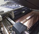
Further to its new module line generation SCHMID InfinityLine and the "New Etching Options" (NEO) the SCHMID Group will present another highlight at the productronica 2015: its optimized NTwC Electro Plater. "NTwC" stands for "New Transport with Clamping" and designates the innovative way of contactfree, horizontal transport of printed circuit boards, during which these are mounted in clamping frames and are transported fully automatically through the system. This transport is particularly gentle and represents a significant advantage in processing, especially for the sensitive UTCs (Ultra Thin Cores) as well as for printed circuit boards with resist pattern.
The SCHMID NTwC Electro Plater has a very wide range of application and can be used, for instance, for Flash Plating, Panel Plating, Pattern Plating, Via Filling, SAP and mSAP. Printed circuit boards with high aspect ratio (> 20:1) and considerably finer substrates (down to 25 microns) can be processed with it, and on the other hand also printed circuit boards with a thickness of up to 3.2mm. Thus, the NTwC Electro Plater proves to be a universally usable solution for the processes of galvanic metallization.
Since SCHMID has considerably reduced the use of moving parts during the revision of the Electro Plater, the system requires only minimum maintenance. Further advantages of the NTwC Electro Plater are its particularly uniform surface distribution of the copper deposit as well as the excellent durability and the height adjustability of the anodes in the module.
For the innovative gate technology of the NTwC Electro Plater, SCHMID has developed a new clamping frame. Its symmetrical contacting ensures a particularly homogeneous electric field, which allows an extremely uniform copper deposition. The proven surge technique of the SCHMID Group, which is appreciated by our customers, as well as the frequency controlled pumps ensure an extremely efficient exchange of the electrolyte.
SCHMID's newly developed clamping frame with symmetrical contacting
Transport of a printed circuit board through the SCHMID NTwC Electro Plater
Share on:


Suggested Items
Designer’s Notebook: What Designers Need to Know About Manufacturing, Part 2
04/24/2024 | Vern Solberg -- Column: Designer's NotebookThe printed circuit board (PCB) is the primary base element for providing the interconnect platform for mounting and electrically joining electronic components. When assessing PCB design complexity, first consider the component area and board area ratio. If the surface area for the component interface is restricted, it may justify adopting multilayer or multilayer sequential buildup (SBU) PCB fabrication to enable a more efficient sub-surface circuit interconnect.
Insulectro’s 'Storekeepers' Extend Their Welcome to Technology Village at IPC APEX EXPO
04/03/2024 | InsulectroInsulectro, the largest distributor of materials for use in the manufacture of PCBs and printed electronics, welcomes attendees to its TECHNOLOGY VILLAGE during this year’s IPC APEX EXPO at the Anaheim Convention Center, April 9-11, 2024.
ENNOVI Introduces a New Flexible Circuit Production Process for Low Voltage Connectivity in EV Battery Cell Contacting Systems
04/03/2024 | PRNewswireENNOVI, a mobility electrification solutions partner, introduces a more advanced and sustainable way of producing flexible circuits for low voltage signals in electric vehicle (EV) battery cell contacting systems.
Heavy Copper PCBs: Bridging the Gap Between Design and Fabrication, Part 1
04/01/2024 | Yash Sutariya, Saturn Electronics ServicesThey call me Sparky. This is due to my talent for getting shocked by a variety of voltages and because I cannot seem to keep my hands out of power control cabinets. While I do not have the time to throw the knife switch to the off position, that doesn’t stop me from sticking screwdrivers into the fuse boxes. In all honesty, I’m lucky to be alive. Fortunately, I also have a talent for building high-voltage heavy copper circuit boards. Since this is where I spend most of my time, I can guide you through some potential design for manufacturability (DFM) hazards you may encounter with heavy copper design.
Trouble in Your Tank: Supporting IC Substrates and Advanced Packaging, Part 5
03/19/2024 | Michael Carano -- Column: Trouble in Your TankDirect metallization systems based on conductive graphite or carbon dispersion are quickly gaining acceptance worldwide. Indeed, the environmental and productivity gains one can achieve with these processes are outstanding. In today’s highly competitive and litigious environment, direct metallization reduces costs associated with compliance, waste treatment, and legal issues related to chemical exposure. What makes these processes leaders in the direct metallization space?