


 Dan’s Biz Bookshelf: ‘Abundance: How We Build a Better Future’
 Trouble in Your Tank: In Complex Systems, Design Rules Aren’t Optional
 It’s Only Common Sense: The Phone Is Still Your Competitive Advantage


Advanced Copper Foil (ACF) to Display Full Line of Circuit Foil Copper Foils at IPC APEX 2016
March 8, 2016 | Advanced Copper FoilEstimated reading time: 2 minutes
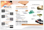
Having signed an exclusive distribution agreement with Circuit Foil Luxemburg in 2015, ACF is now fully ready to provide value-added copper foil products to all regions of the United States and Canada.
ACF welcomes customers and will be exhibiting its full line of Circuit Foil Copper Foils and Aluminum Supported Copper Foils at the IPC/APEX Show in Las Vegas March 15-17, Booth 447.
Foils for the PCB Manufacturer
On display will be standard shiny foils, high bond/Polyimide foil, low loss, ultra-low loss and HVLP foils. There will be a complete display of LP, VLP, HVLP and foils with “Almost No Profile” (Rz ≤ 1.3um). ACF also offers a host of specialty foils for PTFE, Flexible Circuits, ultra-thin foils (≤ 2um) and foils specially designed for High Speed Low Loss Laminates.
Copper Foil with Aluminum Carrier
See both the AFC2, Single-sided Aluminum, and the ACF3, Double-sided Copper Aluminum Copper layers. Manufactured in a clean-room, the ACF family of products guarantee a pristine copper surface, free of debris and other foreign materials. These products also protect the copper surface from epoxy spots and finger prints during the Multilayer Layup process. The unique process, established with complete cleanliness in mind, does not require aluminum shearing during the manufacturing process as others products do. This in conjunction with our unique tooling and proprietary panel cleaning processes allows ACF to guarantee our customers the highest quality panels without the concern of aluminum particles or other foreign materials, with any tooling configuration required.
Special Shielding and Battery Foils
Complete line of foils for industrial markets such as battery and shielding, as well as our foils for PCB application.
About ACF
Advanced Copper Foil is a company dedicated to High Performance Copper Foils and their applications in the Printed Circuit and Battery Shielding Industries. ACF2 and ACF3 aluminum supported foils are products that facilitate the PCB layup process, improve efficiencies and provide a carrier for ultra-thin foils. We are committed to providing PCB Fabricators, Laminate Manufacturers and Battery Shielding Companies with a cost-effective alternative to the traditional products on the market today.
For further information visit: www.advancedcopperfoil.com
Share on:


Testimonial
"We’re proud to call I-Connect007 a trusted partner. Their innovative approach and industry insight made our podcast collaboration a success by connecting us with the right audience and delivering real results."
Julia McCaffrey - NCAB GroupSuggested Items
Driving Innovation: Selecting the Right Laser Source
04/28/2026 | Simon Khesin -- Column: Driving InnovationWhen I first joined Schmoll Maschinen, I brought experience from almost every PCB process, except for laser. As I immersed myself in laser processing, I realized why it can seem so daunting to a newcomer. The complexity arises from three intersecting factors: A vast variety of laser sources: CO2, UV-nano, green-pico, UV-pico, IR-pico, and others; a diverse range of applications: Drilling, cutting, ablation, and more; and an extensive list of materials: These have vastly different absorption rates. Choosing the right machine or laser source is rarely trivial. Even for experienced engineers, answering "Which source is best?" requires examining the business's specific goals.
Institute of Circuit Technology Spring Seminar 2026: A Bright Future in Europe
04/23/2026 | Pete Starkey, I-Connect007Through the leafy lanes and spring flowers of Warwickshire and back to Meridan, the traditional centre of England, and now officially part of the Metropolitan Borough of Solihull in the county of the West Midlands, I attended the Annual General Meeting and Spring Seminar of the Institute of Circuit Technology (ICT) on April 14. Out of the AGM came notable changes in leadership at the top of the Institute: the retirement of Mat Beadel as chair and Emma Hudson as technical director. Effective May 1, Steve Driver is the new chair, and Alun Morgan is the new technical director.
ACCM Unveils Negative and Near-zero CTE Materials for Large-Format AI Chips
04/21/2026 | Advanced Chip and Circuit MaterialsAdvanced Chip and Circuit Materials, Inc. (ACCM) has launched two new materials: Celeritas HM50, with a negative coefficient of thermal expansion (CTE) of -8 ppm/°C to offset the positive CTE and expansion of copper with temperature on circuit boards, and Celeritas HM001, with near-zero CTE and the low-loss performance needed for high-speed signal layers to 224 Gb/s and faster in artificial intelligence (AI) circuits.
Fresh PCB Concepts: Designing PCBs for Harsh Environments—Reliability Is Engineered Upstream
04/23/2026 | Team NCAB -- Column: Fresh PCB ConceptsWhen engineers hear the phrase “harsh environment,” they usually think of the extreme temperature swings, vibration and shock, pressure changes, or radiation in aerospace. However, aerospace is not the only harsh environment where electronic assemblies must survive. Automotive power electronics, downhole oil and gas tools, marine controls, rail systems, defense platforms, and industrial automation equipment all expose PCBs to environments that are equally unforgiving. The stress mechanisms may differ, but the physics does not.
Advanced Packaging for AI: Reliability Starts at the Cu/Cu/Cu Microvia Junction
04/20/2026 | Kuldip Johal, MKS' AtotechThe rapid growth of AI computing, from training clusters to inference at scale, is reshaping demand across the entire electronics supply chain. Advances in technology requirements, such as higher bandwidth, lower latency, and greater compute density, are driving the development of advanced packaging technologies and transforming the PCB industry across design, manufacturing, testing, and even architecture.