Qnity Advances Interconnect Innovations for Next-Generation Smart Consumer Electronics

Qnity Electronics, Inc. introduces ultra-thin flex circuit materials that help enable the next generation of smart consumer electronics, including...
Samsung Electro-Mechanics Signs KRW 360.5 Billion Package Substrate Supply Deal

Samsung Electro-Mechanics has signed a long-term supply agreement (LTA) worth KRW 360.5 billion for 'Memory Semiconductor Package Substrates' with a...
Amkor Technology, NVIDIA Expand AI Infrastructure Partnership
Amkor Technology, Inc., a leading provider of outsourced semiconductor packaging and test services, announced additional investments in South Korea...
NVIDIA, Supply Chain Partners Expand Capacity to Accelerate AI Infrastructure Buildout

NVIDIA announced plans with a group of supply chain partners to expand global manufacturing capacity to meet growing demand for its accelerated...
Hyundai Mobis Advances Korea’s Automotive Semiconductor Collaboration
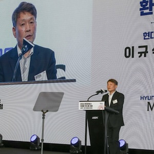
Hyundai Mobis, which has led the way in building Korea's automotive semiconductor ecosystem, is expanding collaboration between the mobility and...
MKS’ Atotech Showcases Advanced PCB Solutions at CPCA Show Plus 2026
MKS Inc., a global provider of enabling technologies that transform our world, announced that its strategic brands Atotech (process chemicals,...

SEMICON West 2026: Another Sold Out Show
October 21, 2026 | Marcy LaRont, I-Connect007

It was a beautiful Fall Day in the heart of downtown San Francisco, as I headed off to the first official day of SEMICON West 2026 on October 13th. Luckily, the beautiful, sunny and crisp Fall weather would endure throughout the week, just as the state was also seeing unprecedented storm activity, flooding and damaging wave activity on the Southern California coast, that juxtaposition in what had once been the only real tech-forward state in the U.S. not lost on me.
Enabling the Interconnect Technologies That Transform Our World: MKS’ Strategic Role in Powering the Future of AI and HPC
October 20, 2026 | John T.C. Lee, with Won Lee, Marc Tricard, and Kuldip Johal
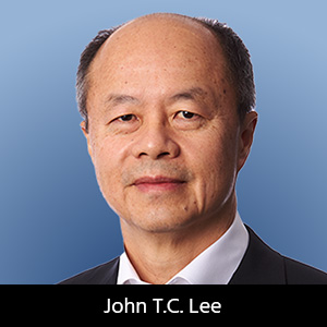
AI is reshaping industries, economies, and daily life at an unprecedented speed. From generative AI and autonomous systems to high-performance computing (HPC) applications in science, defense, and advanced manufacturing, the demand for computational power is accelerating exponentially. But while algorithms capture the spotlight, the true enabler of this transformation lies deeper, in the physical infrastructure that makes AI possible. Performance in the AI era is no longer defined by transistor shrink alone. It is increasingly defined by how efficient systems are integrated, interconnected, cooled, and manufactured at scale.





MORE ARTICLES
Qnity Advances Interconnect Innovations for Next-Generation Smart Consumer Electronics
October 22, 2026 | Qnity
Samsung Electro-Mechanics Signs KRW 360.5 Billion Package Substrate Supply Deal
October 21, 2026 | Samsung Electro-Mechanics
Amkor Technology, NVIDIA Expand AI Infrastructure Partnership
October 21, 2026 | BUSINESS WIRE
NVIDIA, Supply Chain Partners Expand Capacity to Accelerate AI Infrastructure Buildout
October 21, 2026 | Globe Newswire
Hyundai Mobis Advances Korea’s Automotive Semiconductor Collaboration
October 21, 2026 | PRNewswire
MKS’ Atotech Showcases Advanced PCB Solutions at CPCA Show Plus 2026
October 21, 2026 | MKS Inc.
SMTA Renames Event as Microelectronics Packaging & Integration Symposium
October 20, 2026 | SMTA
Fujifilm, ePac Flexible Packaging Announce Global Strategic Partnership
October 20, 2026 | BUSINESS WIRE
Apple Expands US Manufacturing Partnerships with Qnity for iPhone 18 Pro Camera Technology
October 20, 2026 | BUSINESS WIRE
Polar, IC-Link by imec Partner on 8-Inch GaN Manufacturing
October 19, 2026 | Polar Semiconductor, LLC
Testimonial
"Our marketing partnership with I-Connect007 is already delivering. Just a day after our press release went live, we received a direct inquiry about our updated products!"