


 Elementary, Mr. Watson: High Power: When Physics Becomes Real
 The Shaughnessy Report: Watt About Power Integrity?
 Global PCB Connections: Understanding Your Fabricator’s Capabilities (or Niche)


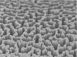
A Tough Coat for Silicon
March 22, 2017 | A*STAREstimated reading time: 2 minutes
A simple, green method that applies a protective coating to semiconductors could help to develop these materials for many applications, from batteries to biosensors.
Silicon forms an oxide layer on its surface when exposed to air or moisture, which can detract from its electronic properties. Adding a ‘skin’ of molecules to the silicon can provide a physical barrier that prevents oxidation, but forming these monolayers can be tricky, requiring an inert atmosphere and long processing times, or demand the use of potentially harmful organic solvents.
Sreenivasa Reddy Puniredd of the A*STAR Institute of Materials Research and Engineering and colleagues have now developed a new way to deliver the protective molecules using supercritical carbon dioxide (scCO2). Carbon dioxide is converted to scCO2 under high pressure, when it becomes a free-flowing liquid that is chemically inert, inexpensive, and more environmentally-friendly than traditional solvents.
The researchers used scCO2 to carry molecules called alkylthiols, which contain long carbon chains with a sulfur atom at one end. Sulfur forms a stable bond with silicon, while the water-repelling carbon chains make a tightly-packed skin on silicon’s surface.
To apply the coating they used alkylthiols containing between seven and 18 carbon atoms to coat silicon, germanium, and silicon nanowires. Each procedure took a few hours, and produced monolayers between 1.6 nanometers and 2.3 nanometers thick that resisted wear and repelled water. The greatest effect was seen for the longest alkylthiol chains.
The monolayers also protected the surface from oxygen for more than 50 days; those prepared using conventional solvents were typically stable for less than seven days. “The increase in stability was expected, but such long-term stability was a surprise,” says Puniredd.
Silicon nanowires are being tested for a range of biological applications, including biosensors and antibacterial surfaces. Although fragile and easily damaged by other monolayer formation methods, the silicon nanowires were undamaged by the scCO2 process, allowing the researchers to test how they interacted with human liver cells. Those protected by the 18-carbon alkylthiol significantly reduced cell growth on the nanowires, compared with unprotected nanowires or a flat silicon surface. This is probably because the cells’ proteins could not latch on to the monolayer’s long carbon chains.
“This scCO2 technology can be adopted for many kinds of inorganic surface modification,” says Puniredd. “The technology is not only scalable, but also enhances the quality and stability of the film. It can potentially replace billions of pounds of organic solvents used every year in thin-film fabrication and cleaning applications.”
Share on:


Testimonial
"Advertising in PCB007 Magazine has been a great way to showcase our bare board testers to the right audience. The I-Connect007 team makes the process smooth and professional. We’re proud to be featured in such a trusted publication."
Klaus Koziol - atgSuggested Items
Beyond Thermal Conductivity: Exploring Polymer-based TIM Strategies for High-power-density Electronics
10/13/2025 | Padmanabha Shakthivelu and Nico Bruijnis, MacDermid Alpha Electronics SolutionsAs power density and thermal loads continue to increase, effective thermal management becomes increasingly important. Rapid and efficient heat transfer from power semiconductor chip packages is essential for achieving optimal performance and ensuring long-term reliability of temperature-sensitive components. This is particularly crucial in power systems that support advanced applications such as green energy generation, electric vehicles, aerospace, and defense, along with high-speed computing for data centers and artificial intelligence (AI).
Driving Innovation: Depth Routing Processes—Achieving Unparalleled Precision in Complex PCBs
09/08/2025 | Kurt Palmer -- Column: Driving InnovationIn PCB manufacturing, the demand for increasingly complex and miniaturized designs continually pushes the boundaries of traditional fabrication methods, including depth routing. Success in these applications demands not only on robust machinery but also sophisticated control functions. PCB manufacturers rely on advanced machine features and process methodologies to meet their precise depth routing goals. Here, I’ll explore some crucial functions that empower manufacturers to master complex depth routing challenges.
Polar Instruments Announces Additive Transmission Line Support for Si9000e
08/20/2025 | Polar InstrumentsTransmission lines embedded into the PCB surface are a feature of UHDI constructions. The 2025 fall release of Polar's Si9000e PCB impedance & insertion loss transmission line field solver incorporates eight new single ended, differential and coplanar transmission line structures.
Henniker Plasma Launches Stratus Turnkey Plasma Manufacturing Cell
08/13/2025 | Henniker PlasmaHenniker Plasma, a leading manufacturer of plasma treatment systems, proudly announces the launch of its Stratus Plasma Manufacturing Cell range — a fully integrated, turnkey solution that combines advanced atmospheric plasma surface treatment with robotic automation.
Trouble in Your Tank: Metallizing Flexible Circuit Materials—Mitigating Deposit Stress
08/04/2025 | Michael Carano -- Column: Trouble in Your TankMetallizing materials, such as polyimide used for flexible circuitry and high-reliability multilayer printed wiring boards, provide a significant challenge for process engineers. Conventional electroless copper systems often require pre-treatments with hazardous chemicals or have a small process window to achieve uniform coverage without blistering. It all boils down to enhancing the adhesion of the thin film of electroless copper to these smooth surfaces.