


 Beyond Design: Skip-layer Routing—The Waveguide Structure That Makes 224G Possible
 Designers Notebook: Old vs. New School System-level Packaging—Flip-Chip to Chiplets
 Elementary, Mr. Watson: Builders of the Dream


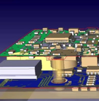
Zuken and Nano Dimension are working together to advance the 3D printing user experience and prototype turnaround times. Nano Dimension, a leader in electronic printing technologies, will take advantage of the support for implementing electronic technologies provided by Zuken’s market-leading, native 3D, system-level design solution, CR-8000 Design Force.
Simon Fried, Chief Business Officer, Nano Dimension, said, “It has been an amazing few years for our company as we’ve fielded interest in our technology. We’re excited about working with Zuken to harness Design Force and take our products even further, giving our users a seamless experience from design to output and optimization.”
Nano Dimension develops advanced 3D printed electronics platforms, including the DragonFly 2020 3D printer for multilayer printed circuit boards, and nanotechnology-based conductive and dielectric inks for their 3D printers. The printer continues to capture global industry and media attention. Future developments will see expansion to support additional board technologies including flexible circuits and embedded components.
Humair Mandavia, Chief Strategy Officer, Zuken USA, said, “Zuken’s CR-8000 Design Force retains all the detailed data needed for 3D printing and allows export direct to manufacturing or 3D printing, without losing integrity. Nano Dimension’s 3D printers are typical of the many applications we envisioned when we pioneered native 3D design for manufacturing.”
Design Force is the sole design tool that allows specification of unique rules for materials, meaning no extra steps are needed when 3D printing to silver and any other future conductive material. Zuken also offers dedicated DFM solutions to support printed electronics via its DFM Inkjet module that optimizes CAD data for inkjet printers. With these solutions from Nano Dimension and Zuken users can expect to spend more time innovating and getting new ideas to market, rather than dealing with design administration.
Movie: Nano Dimension’s DragonFly 2020 3D Printing Platform for Electronics:
About Nano Dimension
Nano Dimension Ltd., founded in 2012, is focused on the research and development of advanced 3D printed electronics, including a 3D printer for multilayer printed circuit boards, and the development of nanotechnology-based conductive and dielectric inks, which are complementary products for 3D printers. Nano Dimension’s novel and proprietary technologies enable the use of conductive and dielectric inks for ultra-rapid prototyping of complex, high-performance multilayer circuit boards. The company’s PCB 3D printer is the result of combining advanced breakthroughs in inkjet technology, 3D printing and nanotechnology.
About Zuken
Zuken is a global provider of leading-edge software and consulting services for electrical and electronic design and manufacturing. Founded in 1976, Zuken has the longest track record of technological innovation and financial stability in the electronic design automation (EDA) software industry. The company’s extensive experience, technological expertise and agility, combine to create world-class software solutions. Zuken’s transparent working practices and integrity in all aspects of business produce long-lasting and successful customer partnerships that make Zuken a reliable long-term business partner.
Zuken is focused on being a long-term innovation and growth partner. The security of choosing Zuken is further reinforced by the company’s people—the foundation of Zuken’s success. Coming from a wide range of industry sectors, specializing in many different disciplines and advanced technologies, Zuken’s people relate to and understand each company’s unique requirements. For more information about the company and its products, visit www.zuken.com.


