


 The Marketing Minute: Marketing With Layers
 The Right Approach: Electro-Tek—A Williams Family Legacy, Part 1
 It’s Only Common Sense: If You’re Not Differentiated, You’re Dead


Laser Empowers 3D Imaging Technique
January 16, 2019 | Chinese Academy of SciencesEstimated reading time: 2 minutes
Three-dimensional (3D) microscopic imaging can help obtain and display stereo information of specimens. Its wide applications cover biological sample observation, tumor diagnostics, material investigation; and various techniques using visible light have been developed to obtain 3D images.
Recently, a research team led by Professor LIU Cheng from Key Laboratory of High Power Laser and Physics, Shanghai Institute of Optics and Fine Mechanics of the Chinese Academy of Sciences, has developed K-domain transform based 3D imaging technique.
By simply illuminating a sample with a light sheet and rearranging the angular frequency components of the reflected light, this technique realizes the measurement of the inner 3D structure.
Researchers adopted a thin light sheet to illuminate the object along the optical axis and recorded both the modulus and phase of the reflected light in the epi-direction with holography. The structure of the illuminated slice could be clearly reconstructed by transforming the spatial components of the reflected light to the light-sheet plane from the lateral recording plane.
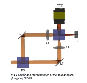
In their experiment, the optical alignment was almost the same as that used for digital holography in reflecting geometry.
To check the axial resolution, a parallel laser beam from a beam splitter passed through the cylindrical lens to form a light sheet to illuminate the sample to be observed.
The reflected light from the sample interfered with another parallel beam to form the offline hologram, which was recorded by a CCD(Charge-coupled Device), and the complex amplitude of the reflected light from the sample can be accurately measured.
Then, the distribution of the sample structure on the light-sheet plane can be calculated as described above. For simplicity, the first sample used in the experiments was a 1.8 mm thick piece of glass. The axial resolution obtained is 90 um.
To verify the performance of the proposed method in generating a 2D image vertical to the light-sheet plane, another set of experiments were carried out.
The thickness of the glass is 1.8 mm. The fabrication of these structures was realized with femtosecond laser processing, and the scale of these circles and crosses was approximately 200 um.
Another experimental results were from a damaged optical filter with an anti-reflection film scratched on both sides, where all the fine scratches are clearly observed. The thickness of the optical filter is 1.8 mm.
These two sets of experimental results match the theoretical expectations well and verify the feasibility of the proposed K-domain transform based 3D imaging method.
To further measure the lateral resolution capability of the proposed method quantitatively, they fabricated a USAF1951 resolution target on one side of a piece of glass and tiny squares with random distribution on its other side.
The material of the tiny bars of the resolution target and the random squares was evaporated SiO2. As seen in Fig. 3, the resolution in the x direction is approximately 4.38 um, and the resolution in the y direction is approximately 5.52 um.
This new technique reconstructs actual 3D image with high-speed and high-resolution, and can apply to rapid detection of optical damage.
Fig. 2 Image reconstructed on axial plane. (Image by SIOM)
Fig.3 Resolution target on one side and tiny squares with random distribution on its other side. (Image by SIOM)
Share on:


Testimonial
"The I-Connect007 team is outstanding—kind, responsive, and a true marketing partner. Their design team created fresh, eye-catching ads, and their editorial support polished our content to let our brand shine. Thank you all! "
Sweeney Ng - CEE PCBSuggested Items
TRI to Unveil New High-Throughput AOI and AXI at productronica 2023
09/15/2023 | TRITest Research, Inc. (TRI), the leading test and inspection systems provider for the electronics manufacturing industry, will join productronica 2023, which will be held at Messe München Center from November 14 – 17, 2023.
UK Space Agency Launches Consultation on Variable Liability Limits for Orbital Operations
09/15/2023 | UK Space AgencyThe proposals from the UK Space Agency follow a review into the UK’s approach to setting the amount of an operator’s liability in licences for orbital operations, a key commitment of the government’s National Space Strategy.
MediaTek Successfully Develops First Chip Using TSMC's 3nm Process, Set for Volume Production in 2024
09/14/2023 | MediaTekMediaTek and TSMC announced that MediaTek has successfully developed its first chip using TSMC's leading-edge 3nm technology, taping out MediaTek’s flagship Dimensity system-on-chip (SoC) with volume production expected next year.
MKS’ Atotech to Participate in IPCA Expo 2023
09/14/2023 | MKS’ AtotechMKS’ Atotech, a leading surface finishing brand of MKS Instruments, will participate in the upcoming IPCA Expo at Bangalore International Exhibition Centre (BIEC) and showcase its latest PCB manufacturing solutions from September 13 – 15.
Comtech Unveils New BRIDGE Solutions to Increase Access to Global Hybrid Connectivity
09/12/2023 | Business WireComtech launched its new blended, resilient, integrated, digital, global, end-to-end (BRIDGE) connectivity solutions. Comtech’s BRIDGE solutions provide portable, adaptable, full-service communications networks that can be established in a matter of hours and help “bridge the gap” for traditional satellite and terrestrial infrastructures.