


 Global PCB Connections: Understanding the General Fabrication Process—A Designer’s Hidden Advantage
 Elementary, Mr. Watson: Why Your PCB Looks Like a Studio Apartment
 The Shaughnessy Report: A Plan for Floor Planning


Breakthrough in Understanding Electrical Conductivity in Doped Organic Semiconductors
February 1, 2019 | TU DresdenEstimated reading time: 2 minutes
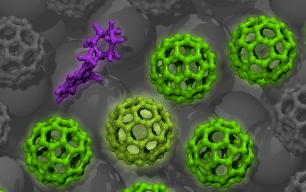
Researchers from the Dresden Integrated Center for Applied Physics and Photonic Materials (IAPP) and the Center for Advancing Electronics Dresden (cfaed) at TU Dresden, in cooperation with Stanford University (USA) and the Institute for Molecular Science in Okazaki (Japan), have identified the key parameters that influence electrical conductivity in doped organic conductors.
Organic semiconductors enable the fabrication of large-scale printed and mechanically flexible electronic applications, and have already successfully established themselves on the market for displays in the form of organic light-emitting diodes (OLEDs). In order to break into further market segments, however, improvements in performance are still needed. Doping is the answer. In semiconductor technology, doping refers to the targeted introduction of impurities (also called dopants) into the semiconductor material of an integrated circuit. These dopants function as intentional "disturbances" in the semiconductor that can be used to specifically control the behaviour of the charge carriers and thus the electrical conductivity of the original material. Even the smallest amounts of these can have a very strong influence on electrical conductivity. Molecular doping is an integral part of the majority of commercial organic electronics applications. Until now, however, an insufficient fundamental physical understanding of the transport mechanisms of charges in doped organic semiconductors has prevented a further increase in conductivity to match the best inorganic semiconductors such as silicon.
Researchers from the Dresden Integrated Center for Applied Physics and Photonic Materials (IAPP) and the Center for Advancing Electronics Dresden (cfaed) at TU Dresden, in cooperation with Stanford University and the Institute for Molecular Science in Okazaki, have now identified key parameters that influence electrical conductivity in doped organic conductors. The combination of experimental investigations and simulations has revealed that introducing dopant molecules into organic semiconductors creates complexes of two oppositely charged molecules. The properties of these complexes like the Coulomb attraction and the density of the complexes significantly determine the energy barriers for the transport of charge carriers and thus the level of electrical conductivity. The identification of important molecular parameters constitutes an important foundation for the development of new materials with even higher conductivity.
The results of this study have just been published in the renowned journal "Nature Materials". While the experimental work and a part of the simulations were conducted at the IAPP, the Computational Nanoelectronics Group at the cfaed under the leadership of Dr. Frank Ortmann verified the theoretical explanations for the observations by means of simulations at the molecular level. In doing so, a comprehensive foundation for new applications for organic semiconductor technology has been created.
About the Computational Nanoelectronics Group
The research group at the Center for Advancing Electronics Dresden (cfaed) headed by Dr. Frank Ortmann investigates electronic properties and the charge transport properties of innovative semiconductor materials. Organic semiconductors are currently at the heart of this research, which is being funded by the German Research Foundation as part of the Emmy Noether Program. The group has been located at cfaed since 2017.
Share on:


Testimonial
"We’re proud to call I-Connect007 a trusted partner. Their innovative approach and industry insight made our podcast collaboration a success by connecting us with the right audience and delivering real results."
Julia McCaffrey - NCAB GroupSuggested Items
Insulectro and Electroninks Sign North American Distribution Agreement
08/12/2025 | InsulectroElectroninks, a leader in metal organic decomposition (MOD) inks for additive manufacturing and advanced semiconductor packaging, today announced a strategic collaboration and distribution partnership with Insulectro, a premier distributor of materials used in printed electronics and advanced interconnect manufacturing.
Happy’s Tech Talk #41: Sustainability and Circularity for Electronics Manufacturing
08/13/2025 | Happy Holden -- Column: Happy’s Tech TalkI attended INEMI’s June 12 online seminar, “Sustainable Electronics Tech Topic Series: PCBs and Sustainability.” Dr. Maarten Cauwe of imec spoke on “Life Cycle Inventory (LCI) Models for Assessing and Improving the Environmental Impact of PCB Assemblies,” and Jack Herring of Jiva Materials Ltd. spoke on “Transforming Electronics with Recyclable PCB Technology.” This column will review information and provide analysis from both presentations.
Dymax Renews Connecticut Headquarters Lease, Reinforces Long-Term Commitment to Local Community
08/08/2025 | DymaxDymax, a global manufacturer of rapid light-curing materials and equipment, is pleased to announce the renewal and extension of its corporate lease at its 318 Industrial Lane, Torrington, headquarters.
EMC Taiwan Receives IPC-4101 Qualified Products Listing Certification
08/08/2025 | Global Electronics AssociationIPC’s Validation Services Program has awarded an IPC-4101 Qualified Products Listing (QPL) to Elite Materials Co. (EMC), an electronics base material manufacturing company headquartered in Taoyuan City, Taiwan.
DuPont Reports Second Quarter 2025 Results
08/06/2025 | PRNewswireNet sales increased 3% led by organic sales growth of 2% which consisted of a 4% increase in volume partially offset by a 2% decrease in price. Currency was a 1% benefit.