-

- News
- Books
Featured Books
- design007 Magazine
Latest Issues
Current Issue
Signal Integrity
If you don’t have signal integrity problems now, you will eventually. This month, our expert contributors share a variety of SI techniques that can help designers avoid ground bounce, crosstalk, parasitic issues, and much more.

Proper Floor Planning
Floor planning decisions can make or break performance, manufacturability, and timelines. This month’s contributors weigh in with their best practices for proper floor planning and specific strategies to get it right.

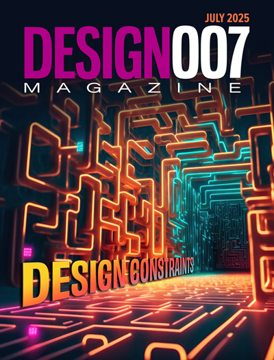
Showing Some Constraint
A strong design constraint strategy carefully balances a wide range of electrical and manufacturing trade-offs. This month, we explore the key requirements, common challenges, and best practices behind building an effective constraint strategy.
- Articles
- Columns
- Links
- Media kit
||| MENU - design007 Magazine
What Does Intelligent Routing Look Like?
November 27, 2019 | Brent Klingforth, Mentor, a Siemens businessEstimated reading time: 1 minute
Many PCB design projects miss schedule commitments by 70% due to delayed routing and lack of automation. Moreover, due to late-stage design changes, schedules are not met, and the addition of those new items takes 10 times longer or more to incorporate than if changes were added from the beginning.
Fortunately, over the past several years, powerful routing capabilities have been added that allow designers to address a number of specific, critical tasks. These automated, intelligent PCB placement and routing technologies can accelerate design cycle times by 50% or more, eliminating issues due to collision and space constraints. By taking advantage of these new routing solutions, designers are three times more likely to achieve first-pass design success and produce quality board designs on time.
To outline what routing automation is, let’s review the four pieces of the puzzle that, when used together, can cut 50% or more of your design cycle time (and even more during design updates) from the simplest to the most complex designs.
1. Design Rules
Design rules are critical for designing a high-quality, robust PCB with automation, whether it’s part placement, creating plane areas, or routing traces. With rules being an instrumental part of PCB design, electrical designers should have access to any rule that can be defined, from the PCB tool to the schematic tool. Limiting rule entry to only the PCB level or partial rules from the schematic delays the development process. This type of system forces the electrical engineer to use antiquated methods of conveying design intent to the layout designer. A proper design flow would allow the electrical engineer to enter critical constraints, such as differential pairs; tuned routes; RF nets; high power; sensitive, low-amplitude analog or digital signals; DDR channels; and more. If they choose to define common constraints, they have that ability as well.
To read this entire article, which appeared in the October 2019 issue of Design007 Magazine, click here.
Testimonial
"Our marketing partnership with I-Connect007 is already delivering. Just a day after our press release went live, we received a direct inquiry about our updated products!"
Rachael Temple - AlltematedSuggested Items
Meet the Author Podcast: Martyn Gaudion Unpacks the Secrets of High-Speed PCB Design
07/16/2025 | I-Connect007In this special Meet the Author episode of the On the Line with… podcast, Nolan Johnson sits down with Martyn Gaudion, signal integrity expert, managing director of Polar Instruments, and three-time author in I-Connect007’s popular The Printed Circuit Designer’s Guide to... series.
Intervala Hosts Employee Car and Motorcycle Show, Benefit Nonprofits
08/27/2024 | IntervalaIntervala hosted an employee car and motorcycle show, aptly named the Vala-Cruise and it was a roaring success! Employees had the chance to show off their prized wheels, and it was incredible to see the variety and passion on display.
KIC Honored with IPC Recognition for 25 Years of Membership and Contributions to Electronics Manufacturing Industry
06/24/2024 | KICKIC, a renowned pioneer in thermal process and temperature measurement solutions for electronics manufacturing, is proud to announce that it has been recognized by IPC for 25 years of membership and significant contributions to electronics manufacturing.
Boeing Starliner Spacecraft Completes Successful Crewed Docking with International Space Station
06/07/2024 | BoeingNASA astronauts Barry "Butch" Wilmore and Sunita "Suni" Williams successfully docked Boeing's Starliner spacecraft to the International Space Station (ISS), about 26 hours after launching from Cape Canaveral Space Force Station.
KIC’s Miles Moreau to Present Profiling Basics and Best Practices at SMTA Wisconsin Chapter PCBA Profile Workshop
01/25/2024 | KICKIC, a renowned pioneer in thermal process and temperature measurement solutions for electronics manufacturing, announces that Miles Moreau, General Manager, will be a featured speaker at the SMTA Wisconsin Chapter In-Person PCBA Profile Workshop.


