


 Learning with Leo: Drones—Meeting Demand Without Compromise
 Nolan’s Notes: Our Spotlight on North America
 Global Sourcing Spotlight: Building a Supply Chain That Bends, Not Breaks


AltiumLive Frankfurt 2019: Happy Holden Keynote
December 12, 2019 | Pete Starkey, I-Connect007Estimated reading time: 5 minutes
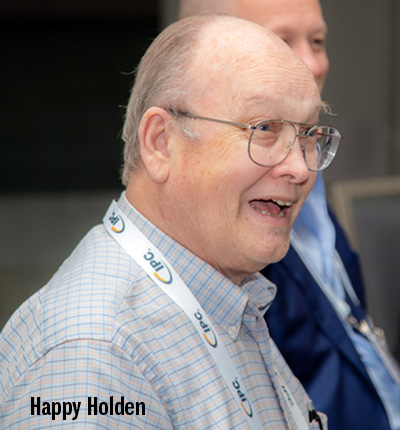
Nobody left early! Altium had wisely kept Happy Holden’s keynote presentation on “PCB Trends that Will Impact Your Future” until the end of the final day of the AltiumLive 2019 European PCB Design Summit in Frankfurt, Germany. Everyone was crowded into the Congress Center at Frankfurt’s Airport Sheraton, eager to learn from and get inspired by the wisdom of a distinguished luminary in our industry, celebrating over 47 years of experience in leading technical positions worldwide and known as the father of high-density interconnect.
Holden’s advance information set the scene: “Times are rapidly changing. There are some trends of change that will impact printed circuit design, fabrication, and assembly/test. I will briefly talk about three of these trends in this presentation.” He continued: “The crystal ball is a little cloudy about when, but it's coming in your future.” He could even have stolen some words from Bob Dylan, and added, “And you better start swimmin', or you'll sink like a stone.”
Holden held the audience enthralled for over an hour with fascinating stories, shrewd observations, and knowledgeable predictions, interlaced with reminiscences and humorous interludes. His first topic was true factory automation, the coming of the smart factory, taking the achievements of Whelen Engineering as his primary example—a PCB factory with no production workers—a first in North America and probably in the world. The original in-house shop, commissioned in 2015, had been configured for the efficient and cost-effective manufacture of double-sided, multilayer, metal-backed, and rigid-flex boards with an economical batch size of one and a very short process cycle.
The shop achieved a turnaround time of 205 minutes from the issue of material until finished boards were ready for shipping. And the cost was half the price of volume product imported from China and one-tenth of the price for prototypes, all available on two-day delivery. Yields were 99.8%, and there were 50% fewer manufacturing steps, 70% recycling of chemistry, and zero effluent. The return on investment was 56%, with a payback period of fewer than two years.
Such was the success of the in-house shop that Whelen built a larger factory to service the outside market, operating under GreenSource Fabrication, on Industry 4.0 principles. The capability was impressive: imaging down to five-micron lines and spaces, and layer counts up to 36 layers, with controlled impedance better than ±2%, and every trace characterised in three dimensions. A total of 17 technicians managed the whole manufacturing operation 24/7, and Holden reckoned that the factory could easily be run lights-out.
Holden illustrated the factory layout and showed photographs of the equipment, most of which had been manufactured in Europe and specifically designed for its purpose in GreenSource. Everything had code-readers, and every panel had its own unique identity and total traceability. In-line metrology enabled product monitoring and control at every stage, not just dimensions and registration but all of the plating and etching parameters, including throwing power, copper distribution, and etching uniformity. There were several unique proprietary features to the processes and equipment.
Chemical processes were continuously analysed and replenished, including regeneration stages, with very narrow control limits giving effectively steady-state operation. Everything possible was recycled, bought-in chemistry costs were very low, and water consumption was minimal. There was zero effluent as well as greatly reduced cycle times and manufacturing costs, and significant improvements in capability, quality, and traceability. Further, a key benefit of implementing these technologies was sustainability, particularly with regard to a substantially reduced regulatory burden, making it possible to set up PCB fabrication shops in areas without access to water. Because there were no production workers, there was no need for recruitment or training. Improved handling technology enabled thinner and larger-format materials to be processed, and machine-learning loops enabled predictive modelling for achieving tighter tolerances.
Holden’s second topic was digitization for the smart factory. He summarised a typical present-day situation: a fabricator in high-mix manufacturing, servicing the requirements of hundreds of active customers with technologies ranging from standard multilayer through HDI and SLP, and maybe flexible, with no consistency in the format in which customer data was supplied, whether it fit their manufacturing capability or approval status, or whether any design-for-manufacture issues required to be resolved, all of which put additional workload on the front-end system and could cause unnecessary delay.
Holden reviewed the progress of automated data transfer since the 1970s, when it was all on film and paper, until the present day, when the majority of the manufacturing data could be transmitted in IPC-2581 format, although this did not cover information like material specifications, approvals, and regulatory and acceptance specifications. IPC standards were not yet in digital format, although progress was being made.
With Factory 4.0 in prospect, what was needed to universally meet the requirements of the design engineer, the component engineer, supplier, procurement, and manufacturing was a single XML file following a single digital thread for data and process.
IPC’s recently introduced IPC-2591, open-source Connected Factory Exchange standard (CFX) is being widely adopted, giving the electronics industry a means of seamless data communication that could be used to facilitate the implementation of Industry 4.0 and smart factory applications to their manufacturing operations. Complete SMT assembly lines using IPC CFX will be demonstrated at productronica in Munich, IPC APEX EXPO in San Diego, and CPCA in Shanghai. For setting up machines, it would be necessary to develop digital recipes similar to those already established in the semiconductor industry for equipment-to-host data communications. Their standardised interface protocol, known as SECS/GEM (SEMI Equipment Communications Standard/Generic Equipment Model), was different from IPC-2591 but could be driven from IPC-2581.
Holden concluded his presentation with a discussion of how artificial intelligence could affect design tools. He set the scene with an illustration from Intel, which announced that the journey to the intelligent factory would depend upon the integration of information technology systems used for data-centric computing with operational technology systems used to monitor events, processes, and devices in a culture prepared for the introduction of AI.
Traditionally, product development followed a sequential “over the wall” progression. Designers worked in isolation, and, eventually, manufacturing had to assemble the product: “We designed it, you build it!” Typically, the product was not designed to suit the manufacturing processes, and it was too late to make changes. This was before the concept of design for manufacturing (DFM), which had been pioneered during Holden’s career at Hewlett-Packard as long ago as 1988, although it was not made public at that time.
Board Construction Advisor, a software version of HP’s DFM manual, had been developed in 1991 with the objective of lowering the costs of printed circuits and specifying the physical design to meet manufacturing requirements and performance goals. In 1994, HP Laboratories’ Design Explorer explained parametric design generation and analysis and gave a framework for representation and use of engineering information, specifying the design task directly in terms of constraints and goals. It featured interactive constraint checking and propagation, automatic search for and generation of realisable PCB designs, and support for interactive multi-criteria, multi-objective optimisation, and trade-off analysis.
The only published information, dated 1994, described it as a parametric design assistant for concurrent engineering, which provided an exemplar of synergistic combination of AI and human interface technologies. But it still needed an experienced human designer to make decisions about what was best, and it had been necessary to feed it with over 200 designs of varying complexity in order for it to learn.
All of that was 25 years ago, so how could artificial intelligence affect PCB design tools of the future? Holden commented that electronics would advance even faster than before, so the design community must be ready. Maybe AI would come to the rescue? Intel had recently launched its new Spring Hill processor—Nervana Neural Network Processor for Inference, or Intel Nervana NNP-I—designed for AI. Could this be the beginning of a new era?
Happy Holden has boundless knowledge and packed so much information into the final hour of the AltiumLive 2019 PCB Design Summit that it was difficult to absorb it all. I trust that my notes give some indication of the salient points of a spectacular presentation.
Share on:


Testimonial
"In a year when every marketing dollar mattered, I chose to keep I-Connect007 in our 2025 plan. Their commitment to high-quality, insightful content aligns with Koh Young’s values and helps readers navigate a changing industry. "
Brent Fischthal - Koh YoungSuggested Items
Driving Innovation: Selecting the Right Laser Source
04/28/2026 | Simon Khesin -- Column: Driving InnovationWhen I first joined Schmoll Maschinen, I brought experience from almost every PCB process, except for laser. As I immersed myself in laser processing, I realized why it can seem so daunting to a newcomer. The complexity arises from three intersecting factors: A vast variety of laser sources: CO2, UV-nano, green-pico, UV-pico, IR-pico, and others; a diverse range of applications: Drilling, cutting, ablation, and more; and an extensive list of materials: These have vastly different absorption rates. Choosing the right machine or laser source is rarely trivial. Even for experienced engineers, answering "Which source is best?" requires examining the business's specific goals.
Institute of Circuit Technology Spring Seminar 2026: A Bright Future in Europe
04/23/2026 | Pete Starkey, I-Connect007Through the leafy lanes and spring flowers of Warwickshire and back to Meridan, the traditional centre of England, and now officially part of the Metropolitan Borough of Solihull in the county of the West Midlands, I attended the Annual General Meeting and Spring Seminar of the Institute of Circuit Technology (ICT) on April 14. Out of the AGM came notable changes in leadership at the top of the Institute: the retirement of Mat Beadel as chair and Emma Hudson as technical director. Effective May 1, Steve Driver is the new chair, and Alun Morgan is the new technical director.
ACCM Unveils Negative and Near-zero CTE Materials for Large-Format AI Chips
04/21/2026 | Advanced Chip and Circuit MaterialsAdvanced Chip and Circuit Materials, Inc. (ACCM) has launched two new materials: Celeritas HM50, with a negative coefficient of thermal expansion (CTE) of -8 ppm/°C to offset the positive CTE and expansion of copper with temperature on circuit boards, and Celeritas HM001, with near-zero CTE and the low-loss performance needed for high-speed signal layers to 224 Gb/s and faster in artificial intelligence (AI) circuits.
Fresh PCB Concepts: Designing PCBs for Harsh Environments—Reliability Is Engineered Upstream
04/23/2026 | Team NCAB -- Column: Fresh PCB ConceptsWhen engineers hear the phrase “harsh environment,” they usually think of the extreme temperature swings, vibration and shock, pressure changes, or radiation in aerospace. However, aerospace is not the only harsh environment where electronic assemblies must survive. Automotive power electronics, downhole oil and gas tools, marine controls, rail systems, defense platforms, and industrial automation equipment all expose PCBs to environments that are equally unforgiving. The stress mechanisms may differ, but the physics does not.
Advanced Packaging for AI: Reliability Starts at the Cu/Cu/Cu Microvia Junction
04/20/2026 | Kuldip Johal, MKS' AtotechThe rapid growth of AI computing, from training clusters to inference at scale, is reshaping demand across the entire electronics supply chain. Advances in technology requirements, such as higher bandwidth, lower latency, and greater compute density, are driving the development of advanced packaging technologies and transforming the PCB industry across design, manufacturing, testing, and even architecture.