


 Beyond Design: Skip-layer Routing—The Waveguide Structure That Makes 224G Possible
 Designers Notebook: Old vs. New School System-level Packaging—Flip-Chip to Chiplets
 Elementary, Mr. Watson: Builders of the Dream


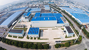
Ventec International Group Co., Ltd. has significantly increased its PTFE laminate manufacturing capabilities following a strategic investment in a new state-of-the-art high-temperature press and lay-up/break-down line at its Suzhou (China) manufacturing plant.
With 5G and evermore sophisticated radar applications, the demand and requirements for low loss/high frequency material is accelerating. Critical RF/Microwave-, antenna-, power amplifier- and sub-assembly-applications require superior electrical performance that can be delivered through PTFE laminates. To serve the increasing demand of these PTFE type products, Ventec has strengthened its investment in its Suzhou manufacturing plant to be even better positioned for the increase in demand and meet customers accelerated radar and 5G deployment requirements.
The most recent important equipment investment in a new state-of-the-art high-temperature press and lay-up/break-down line at Ventec’s Suzhou (China) manufacturing plant delivers a significant increase in manufacturing capacity to meet the growing demand for PTFE laminates. This includes the launch and roll-out of tec-speed 30.0 - Ventec’s latest ceramic filled high-speed/high-frequency PTFE material range that offers the highest signal-integrity characteristics for the most advanced high-frequency systems such as 77~79 GHz automotive radar systems.
tec-speed 30.0 (VT-3703) offers:
- Dk 3.0 with extremely low Df (0.0009)
- DK-stability versus temperature
- Lower in-plane thermal expansion
The current Dk 3.0 tec-speed 30.0 version will be supplemented by Dk 6.15 and Dk 10.2 versions in the first half of 2020, offering an even wider range of options for applications such as automotive radar, cellular base stations, power amplifiers & antennas, global positioning satellite antennas, patch antennas for wireless communication or power backplanes.
Jason Chung, CEO said: "The investment and installation of the PTFE manufacturing line is yet another important piece of the puzzle in our global growth program. The addition of the line to our range of capabilities demonstrates to our customers our commitment to maintaining the most up-to-date manufacturing technologies that support our clients’ PCB design, development and manufacturing needs."
For more information about Ventec's solutions and the company’s wide variety of products, please visit www.venteclaminates.com.
About Ventec International Group
Ventec International Group Co., Ltd. (6672 TT) is a premier supplier to the Global PCB industry. With volume manufacturing facilities in Taiwan and China and distribution locations and manufacturing sites in both the US and Europe, Ventec specializes in advanced copper clad glass reinforced and metal backed substrates. Ventec materials, which include high-quality enhanced FR4, high-speed/low-loss- & high-performance IMS material technology and an advanced range of thermal management solutions, are manufactured by Ventec using strict quality-controlled processes that are certified to AS9100 Revision D, IATF 16949:2016 and ISO 9001:2015, and are backed by a fully controlled and managed global supply chain, sales- and technical support-network.


